


 Target Condition: Signal Integrity Without Borders
 Elementary, Mr. Watson: PCB Education in the Midst of the Storms
 Beyond Design: How Signals Survive the Hostile PCB Environment


Avishtech, Inc., a simulation-based design software provider headquartered in San Jose, CA, has announced the introduction of its Gauss suite of software for the design and simulation of printed circuit board (PCB) stack-ups and transmission lines used in PCBs and semiconductors.
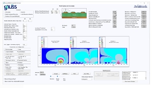
The product suite includes Gauss Stack, a stack-up simulation tool that can build a printed circuit board stack-up with basic components, such as reinforcements and matrix information, and enables the user to perform thermomechanical simulations that include solving for dimensional stability (deformation) during processing, and predicting mechanical and thermal properties. In addition to thermomechanical modeling, Gauss Stack has in-built functionality for avoiding pitfalls associated with resin starvation and glass stop, which can lead to CAF (Conductive Anodic Filamentation) and delamination failures. Gauss Stack goes beyond even these new unique capabilities by calculating the impedance for the entire stack-up in one go in a matter of minutes, through its internal Gauss 2D engine.
The Gauss line of simulation software products also includes Gauss 2D, a high order finite difference method-based 2D field solver for transmission lines in PCBs and semiconductors. Gauss 2D is capable of using basic geometric inputs as they relate to the transmission lines and dielectrics (e.g. width, height, etc.) and performs 2D electromagnetic simulations to predict impedance, RLGC, effective dielectric properties, losses, and more. The user does not need to construct the geometry, as is required by many competitive finite element-based software tools, making the process much faster and easier, all while maintaining exceptional accuracy, since Gauss 2D does the hard work on the user’s behalf. Moreover, Gauss 2D allows the user to perform synthesis, by flipping the problem to solve for the trace width given a target impedance, a unique technological innovation not found in competitive offerings.
The key features of Gauss Stack include:
- Dimensional stability (deformation) prediction
- Prediction of coefficients of thermal expansion in X, Y, and Z directions, in addition to the compliance matrix components (i.e. moduli in different directions), which are inputs for reliability prediction models related to plated through holes and solder joint cycles to failure. This information is critical to avoiding serious failure modes and has, so far, not been available a priori through other means.
- Warnings for resin starvation and glass stop to assist in stack-up design for reliability
- Synthesis and analysis capability for impedance for the full stack-up using the Gauss 2D engine, with up to 3 single ended and 3 differential transmission lines per layer
The key features of Gauss 2D include:
- A high order finite difference and high order integration-based engine for very high accuracy
- Electric potential and field visualization
- Predefined transmission line geometries, covering virtually any configuration (hundreds of combinations, including dual-dielectrics, multiconductor, differential, trapezoidal traces, etc.)
- Synthesis capability for calculating trace width given a target impedance
- Dielectric anisotropy, which enables the user to specify the Dk and DF in both parallel and perpendicular directions
Keshav Amla, Chief Executive Officer, noted, “I am very excited at the release of our new Gauss line of simulation and design products. Gauss Stack and Gauss 2D solve several major pain points for the industry and the products offer functionality that has not been seen before. Gauss Stack provides a drastically simplified workflow that integrates design and full multi-physics simulation into one platform thus reducing a significant amount of wasted effort. The predictions from the tool can help solve/alleviate the problems of scout lots that are sent out just to verify the dimensional characteristics. Additionally, the high fidelity analysis and synthesis capability for impedance, and design for reliability inputs, will really help our customers. Gauss 2D also takes electromagnetic simulations for transmission lines to a new level, through its ability to account for dielectric anisotropy and provide extreme fidelity due to its use of high-order finite-difference schemes, along with high-order integration.”
He added, “Our customers will certainly appreciate the extreme ease-of-use of these products, coupled with the ability to interact with data in a rich user interface, as well as through outputs to standard spreadsheet and data processing software.”
The products are available for evaluation. Interested customers may visit our site for more information: www.avishtech.com
About Avishtech, Inc.
Avishtech, Inc., is a San Jose, CA-based high technology company founded in 2015 on the principle of using a multidisciplinary approach to build the materials-driven technologies of the future. Avishtech’s Gauss line of simulation and design software embodies its long-standing commitment to rigorous and thorough research and development, coupled with its core goal of achieving the highest levels of performance and reliability. Avishtech’s ongoing ventures also include major innovations in autonomous driving, as well as advanced materials development. For more information about Avishtech and its products, please visit www.avishtech.com.


