


 Target Condition: Signal Integrity Without Borders
 Elementary, Mr. Watson: PCB Education in the Midst of the Storms
 Beyond Design: How Signals Survive the Hostile PCB Environment


Zuken announces the availability of eCADSTAR release 2020. With the new release, available configurations of Zuken’s new internet connected PCB design platform, eCADSTAR, have been extended to include new modules for signal integrity, power integrity and IBIS-AMI simulation.
The new modules eCADSTAR Signal Integrity, eCADSTAR Signal Integrity Advanced, eCADSTAR Power Integrity and eCADSTAR IBIS-AMI complement eCADSTAR’s connected PCB design capabilities with powerful analysis tools, such as embedded signal integrity simulation in eCADSTAR Schematic and PCB Editors for pre- and post-layout simulation.
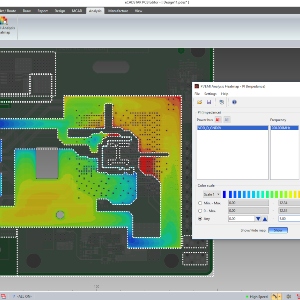
All analysis tools are tightly integrated with eCADSTAR’s comprehensive PCB constraint management and optimization functionality. Results are displayed in a common Analysis Result Viewer within the eCADSTAR design environment. Heatmaps can also be displayed directly within the eCADSTAR PCB editor from the Power Integrity application.
“As products become more complex and faster, analysis becomes a key part of the design process to ensure correct operation. High-speed components and interfaces are at the heart of today’s smart and internet-connected products, and they demand advanced pre- and post-layout analysis for correct operability”, says Markus Bücker, Development Manager, Zuken EMC Technology Center, Paderborn. “eCADSTAR delivers those capabilities in an easy to use embedded environment so that both engineers and PCB designers can deliver exceptional high-speed design quality first time right based on Zuken’s proven technology.”
Signal Integrity
With eCADSTAR Signal Integrity, engineers can plan and check signal integrity throughout the Schematic and PCB layout process. eCADSTAR Signal Integrity Advanced comprises TDR analysis as well as S-Parameter analysis. Simulations can be initiated from eCADSTAR’s Constraint Browser, Electrical Editor, or directly from the eCADSTAR PCB Editor. The simulation Results Viewer is available throughout the eCADSTAR design flow with a consistent user interface. Signal integrity simulation not only makes sure that high-speed signals arrive in good shape: A board with good signal integrity is more resistant to external noise and less likely to consume excess power.
Power Integrity and EMI
Using the eCADSTAR Electromagnetic Interference (EMI) analysis capabilities, engineers can identify the most significant EMI contributors on the board, including differential-mode EMI, common-mode EMI, and power bus noise. If these parameters are optimized during board layout, the electric interference of a design can be kept as low as possible.
With eCADSTAR’s Power Integrity tools, engineers can check AC behavior of the Power Delivery Network (PDN) and ensure DC continuity from power sources to component power inputs and then back where it came from. DC analysis results include current- and voltage distributions across the supply system, pin-to-pin resistance analysis, IR-drop analysis for all supply pins, and identifies current stressed Vias within the supply path.
IBIS-AMI
AMI analysis goes beyond traditional waveform simulation. AMI simulation is most valuable when transceivers include features that cannot be modeled by analog electrical descriptions alone. A traditional IBIS model is an electrical description of buffer driving and receiving characteristics, not including any DSP behavior like that present in PCI Express Gen3 onwards or DDR5. AMI models include this behavior, so engineers can adjust parameters to optimize I/O channels for maximum performance. As with other kinds of simulation, AMI models become even more valuable when you push density and speed envelopes and ultra-high-speed Serializer/Deserializer (SerDes) circuits are closely packed with other parts of your designs. The analysis results will be displayed as an eye diagram and a bathtub curve to check BER (Bit Error Rate) compliance.


