-

- News
- Books
Featured Books
- design007 Magazine
Latest Issues
Current Issue
Signal Integrity
If you don’t have signal integrity problems now, you will eventually. This month, our expert contributors share a variety of SI techniques that can help designers avoid ground bounce, crosstalk, parasitic issues, and much more.

Proper Floor Planning
Floor planning decisions can make or break performance, manufacturability, and timelines. This month’s contributors weigh in with their best practices for proper floor planning and specific strategies to get it right.

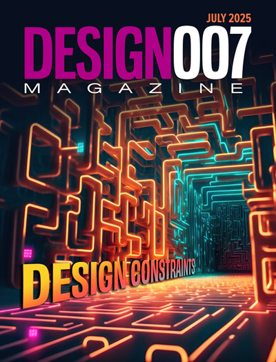
Showing Some Constraint
A strong design constraint strategy carefully balances a wide range of electrical and manufacturing trade-offs. This month, we explore the key requirements, common challenges, and best practices behind building an effective constraint strategy.
- Articles
- Columns
- Links
- Media kit
||| MENU - design007 Magazine
The Magnitude of Stackup Considerations
March 1, 2021 | Michael R Creeden, CID+, MIT, InsulectroEstimated reading time: 1 minute
When I was asked to write about stackup creation, I paused at the magnitude of this subject. It is similar to the framework used to pour concrete cement—you need to get the framework right because the framework has such a big impact on the final outcome. Such is the case with shaping the success or failure of our circuits. In writing the newest training manual due out early this year, I observed that the longest chapter in the textbook was dedicated to this subject.
Therefore, I believe it is truly one of the most important and far-reaching subjects in our industry. It was at the heart of my decision to accept an offer to work for Insulectro because it allows me to make a difference in our industry on this subject. Because it’s such a vast topic, I can only scratch the surface in an article, but I hope to scratch it well.
I always like to remind readers to pursue all printed circuit engineering issues from three simultaneous perspectives when we design for X:
1. DFS—Solvability
Place and route dense critical circuitry to define optimal features and implementing constraints that meet three perspectives. Also, mastering an EDA CAD tool is a significant challenge compounded by accelerated development schedules.
2. DFP—Performance
Ensure that all SI, EMI, and thermal performance metrics are met. You can solve a complicated design, then build a perfect bare board, but if the signal energy does not go where it should, you can throw the board in the trash can.
3. DFM—Manufacturability
As our circuits become more advanced so do the challenges associated with building a bare board. With decreased feature sizes, the tolerance window becomes more precise. Therefore, the layout professional must be aware of the manufacturing capabilities and engage with their supply chain at the beginning of layout. The practice of selecting your supply chain once layout is complete is a flawed approach.
To read this entire article, which appeared in the January 2021 issue of Design007, click here.
Testimonial
"Our marketing partnership with I-Connect007 is already delivering. Just a day after our press release went live, we received a direct inquiry about our updated products!"
Rachael Temple - AlltematedSuggested Items
Meet the Author Podcast: Martyn Gaudion Unpacks the Secrets of High-Speed PCB Design
07/16/2025 | I-Connect007In this special Meet the Author episode of the On the Line with… podcast, Nolan Johnson sits down with Martyn Gaudion, signal integrity expert, managing director of Polar Instruments, and three-time author in I-Connect007’s popular The Printed Circuit Designer’s Guide to... series.
Intervala Hosts Employee Car and Motorcycle Show, Benefit Nonprofits
08/27/2024 | IntervalaIntervala hosted an employee car and motorcycle show, aptly named the Vala-Cruise and it was a roaring success! Employees had the chance to show off their prized wheels, and it was incredible to see the variety and passion on display.
KIC Honored with IPC Recognition for 25 Years of Membership and Contributions to Electronics Manufacturing Industry
06/24/2024 | KICKIC, a renowned pioneer in thermal process and temperature measurement solutions for electronics manufacturing, is proud to announce that it has been recognized by IPC for 25 years of membership and significant contributions to electronics manufacturing.
Boeing Starliner Spacecraft Completes Successful Crewed Docking with International Space Station
06/07/2024 | BoeingNASA astronauts Barry "Butch" Wilmore and Sunita "Suni" Williams successfully docked Boeing's Starliner spacecraft to the International Space Station (ISS), about 26 hours after launching from Cape Canaveral Space Force Station.
KIC’s Miles Moreau to Present Profiling Basics and Best Practices at SMTA Wisconsin Chapter PCBA Profile Workshop
01/25/2024 | KICKIC, a renowned pioneer in thermal process and temperature measurement solutions for electronics manufacturing, announces that Miles Moreau, General Manager, will be a featured speaker at the SMTA Wisconsin Chapter In-Person PCBA Profile Workshop.


