-
-
News
News Highlights
- Books
Featured Books
- smt007 Magazine
Latest Issues
Current IssueSpotlight on India
We invite you on a virtual tour of India’s thriving ecosystem, guided by the Global Electronics Association’s India office staff, who share their insights into the region’s growth and opportunities.
Supply Chain Strategies
A successful brand is built on strong customer relationships—anchored by a well-orchestrated supply chain at its core. This month, we look at how managing your supply chain directly influences customer perception.
What's Your Sweet Spot?
Are you in a niche that’s growing or shrinking? Is it time to reassess and refocus? We spotlight companies thriving by redefining or reinforcing their niche. What are their insights?
- Articles
- Columns
- Links
- Media kit
||| MENU - smt007 Magazine
Absolute EMS Announces Groundbreaking Technology for LED, Medical & Automotive from Averatek
March 8, 2021 | Absolute EMS, Inc.Estimated reading time: 1 minute

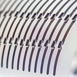
Absolute EMS, Inc., a leading provider of turnkey and consignment manufacturing services, is pleased to announce a new groundbreaking technology for LED, medical and automotive applications from high-tech partner Averatek Corporation. Santa Clara, California based Averatek recently launched Mina™, a chemistry that offers exciting benefits over traditional methods of soldering to Aluminum.
Absolute EMS assembles surface mount components onto polymer substrates with Aluminum traces using Averatek’s Mina™ product. Mina™ is a simple pretreatment for Aluminum that allows soldering to Aluminum as easily as soldering to Copper. It is printed onto the pads using a stencil printer and cured at low temperatures.
Doug Dow, Absolute EMS COO, commented: “It is truly an honor to be in partnership with Averatek. Their mission is to create solutions that deliver ‘tomorrow’s technology’ and this means that together, we are working on things the industry has never seen before. The transparent polymer substrate can be a very thin piece of flexible PET, with flexible Aluminum traces where the components are placed with strategic accuracy. Averatek’s team of PHD’s and Scientists are working with Absolute EMS to continually push the boundaries of science and technology. And this space is where Absolute EMS thrives!”
Averatek’s CEO, Haris Basit, wrote: “It has been wonderful working closely with Absolute EMS on bringing this new capability to the market. Absolute EMS combines the rigor and quality control of an established production facility with a flexibility and openness crucial to developing new products and processes. Finding one organization that encompasses both qualities has greatly accelerated our development cycle.”
Testimonial
"Our marketing partnership with I-Connect007 is already delivering. Just a day after our press release went live, we received a direct inquiry about our updated products!"
Rachael Temple - AlltematedSuggested Items
Trouble in Your Tank: Implementing Direct Metallization in Advanced Substrate Packaging
09/15/2025 | Michael Carano -- Column: Trouble in Your TankDirect metallization systems based on conductive graphite are gaining popularity throughout the world. The environmental and productivity gains achievable with this process are outstanding. Direct metallization reduces the costs of compliance, waste treatment, and legal issues related to chemical exposure. A graphite-based direct plate system has been devised to address these needs.
Closing the Loop on PCB Etching Waste
09/09/2025 | Shawn Stone, IECAs the PCB industry continues its push toward greener, more cost-efficient operations, Sigma Engineering’s Mecer System offers a comprehensive solution to two of the industry’s most persistent pain points: etchant consumption and rinse water waste. Designed as a modular, fully automated platform, the Mecer System regenerates spent copper etchants—both alkaline and acidic—and simultaneously recycles rinse water, transforming a traditionally linear chemical process into a closed-loop system.
Driving Innovation: Depth Routing Processes—Achieving Unparalleled Precision in Complex PCBs
09/08/2025 | Kurt Palmer -- Column: Driving InnovationIn PCB manufacturing, the demand for increasingly complex and miniaturized designs continually pushes the boundaries of traditional fabrication methods, including depth routing. Success in these applications demands not only on robust machinery but also sophisticated control functions. PCB manufacturers rely on advanced machine features and process methodologies to meet their precise depth routing goals. Here, I’ll explore some crucial functions that empower manufacturers to master complex depth routing challenges.
Trouble in Your Tank: Minimizing Small-via Defects for High-reliability PCBs
08/27/2025 | Michael Carano -- Column: Trouble in Your TankTo quote the comedian Stephen Wright, “If at first you don’t succeed, then skydiving is not for you.” That can be the battle cry when you find that only small-diameter vias are exhibiting voids. Why are small holes more prone to voids than larger vias when processed through electroless copper? There are several reasons.
The Government Circuit: Navigating New Trade Headwinds and New Partnerships
08/25/2025 | Chris Mitchell -- Column: The Government CircuitAs global trade winds continue to howl, the electronics manufacturing industry finds itself at a critical juncture. After months of warnings, the U.S. Government has implemented a broad array of tariff increases, with fresh duties hitting copper-based products, semiconductors, and imports from many nations. On the positive side, tentative trade agreements with Europe, China, Japan, and other nations are providing at least some clarity and counterbalance.