


 Target Condition: Signal Integrity Without Borders
 Elementary, Mr. Watson: PCB Education in the Midst of the Storms
 Beyond Design: How Signals Survive the Hostile PCB Environment


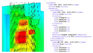
Siemens Digital Industries Software announced the establishment of JEP181—a neutral file, XML-based standard from the JEDEC Solid State Technology Association, which is the global leader in standards development for the microelectronics industry. The JEP181 standard simplifies thermal model data sharing between suppliers and end-users in a single file format called ECXML (Electronics Cooling eXtensible Markup Language).
The new standard was created to meet a significant challenge for electronics manufacturers: as increasingly powerful processors allow companies to pack more performance and functionality into their designs, the effective management of heat dissipation and other thermal factors has become essential to the successful design of their next-generation electronics products. Advanced electronics cooling simulation technologies enable the creation of highly accurate thermal models of new product designs. But the absence of a uniform format for the exchange of thermal simulation data throughout supply chains has created unnecessary duplication of effort and the potential introduction of errors into the stream.
Proposed through the JEDEC JC15 committee, the new JEDEC JEP181 standard simplifies thermal model data sharing. With this universal thermal model sharing standard, electronics manufacturers can reduce the time required to simulate and validate their thermal models.
“The JEP181 standard from JEDEC benefits thermal design engineers by providing wider availability of the key data necessary to validate the thermal performance of today’s advanced designs,” stated Ghislain Kaiser, senior director, Intel Corp. “This standardized format will allow more interoperability between engineering teams, leading to substantial time and cost savings by removing design barriers previously common in thermal engineering.”
Thermal model data availability and sharing is one of the key limiting factors in capitalizing on the benefits of thermal simulation throughout the product design process. Countless hours spent on mining product data sheets for thermal information, or re-implementing 2D engineering drawings within thermal simulation tools, can now be replaced by seamlessly importing commercial 3D simulation tools from software suppliers. The JEP181 standard is ideal for emerging technologies and trends such as miniaturization, 2.5D and 3D semiconductor packaging, and 5G technology-- all of which demand increased power dissipation density.
“As a leader in industrial software solutions, our contribution to the new JEP181 standard can help drive the digitalization of design data to reduce both time and errors for today’s innovative electronics products,” stated Jean-Claude Ercolanelli senior vice president of Simulation and Test Solutions, Siemens Digital Industries Software. “Enabling a seamless digitalized software flow can radically increase the efficiency and accuracy of thermal simulation and thus, enhance the performance and reliability of digital twin prototypes and manufactured products.”


