


 Target Condition: Signal Integrity Without Borders
 Elementary, Mr. Watson: PCB Education in the Midst of the Storms
 Beyond Design: How Signals Survive the Hostile PCB Environment


Zuken is releasing the latest edition of CR-8000, focusing on analysis and reuse. The CR-8000 2021 release features more than 150 enhancements across the tool suite ranging from architectural planning, system-level schematic design and verification, 3D multi-board and advanced packing layout, through to manufacturing outputs generation. The release puts specific emphasis on facilitating improved design efficiency through the benefits of early analysis.
Particular attention in the 2021 release was given to fine-tuning the constraint and simulation capabilities in System Planner and Design Gateway, CR-8000’s engineering front-end applications. As electronic products become more complex, the need for early analysis has become more critical. The 2021 enhancements make marginal design problems more detectable with more robust constraint definition capabilities. For 3D multi-board layout and routing, Design Force users benefit from the new place by area, template, and reuse functionality that enables the application of existing placement and routing patterns on new designs.
Enhanced analog simulation and SI analysis
As part of the early analysis focus, Design Gateway now supports the simulation of PCB parasitic effects in the circuit design stage through the ability to include parasitic element models in SPICE simulations launched directly in the schematic. The simulation model library manager comes in a new, state-of-the-art user interface and is designed to handle today’s volume of model data smoothly. Importing models from various sources such as IBIS, SPICE, or S-Parameters is presented uniformly at the user’s fingertips.
Furthermore, signal integrity (SI) analysis functionality has been enhanced to support the execution of parameter sweeps across multiple pin models in one pass. A user can now explore the most suitable model parameters in a shortened timeframe. In addition, the SI Analysis now considers a more accurate model for the surface roughness of the copper PCB material. The SI verification of differential pair routing now reports measurement results of crossing voltages in both tables and waveform display. User productivity has been further improved by specifying automatic extraction and exporting of PI and EMI analysis results. Time-intensive analysis functions such as the IBIS AMI SerDes are now completed in less time.
Board layout and routing assisted by intelligent template and reuse functionality
Design Force benefits from numerous new functions to help organize and streamline large designs. Users can now guide component placement for large boards based on schematic sheet component positioning. Exact placement and routing patterns from previous designs are reusable on new board designs with a new ‘Create Used Board’ function. By creating specific functions for manual tasks such as creating anti-pads (protected areas around through-holes) or solder resist subtraction, design time is reduced.
Multi-discipline simulation of multi-board systems
The integration of ANSYS simulation tools into CR-8000 Design Force has been extended to cover multi-physics analysis of multi-board designs to enable identification and correction of system-level design integrity issues. This new level of integration will reduce time-consuming and costly redesign efforts in advanced stages of the engineering process. With Design Force 2021, multi-discipline designs can be transferred to ANSYS in a single EDB file for analysis of multi-board designs, including mechanical chassis and enclosure data.
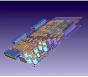
A complete state-of-the-art 3D electronic system design platform
CR-8000 is a complete state-of-the-art 3D electronic system design platform featuring seamlessly integrated applications for architectural planning, detailed engineering, physical layout, MCAD collaboration, and manufacturing optimization. CR-8000 provides a unified environment for designing and verifying single and multi-board systems, including chip-scale packaging (CSP), multi-chip modules, and system-in-package technologies (SiP). CR-8000 is the only PCB design solution complemented by data management capabilities providing comprehensive library, module, configuration, and release management. Utilizing the latest in software and hardware acceleration, CR-8000 can handle the most extensive designs with ease.


