-
- News
- Books
Featured Books
- design007 Magazine
Latest Issues
Current IssueProper Floor Planning
Floor planning decisions can make or break performance, manufacturability, and timelines. This month’s contributors weigh in with their best practices for proper floor planning and specific strategies to get it right.
Showing Some Constraint
A strong design constraint strategy carefully balances a wide range of electrical and manufacturing trade-offs. This month, we explore the key requirements, common challenges, and best practices behind building an effective constraint strategy.
All About That Route
Most designers favor manual routing, but today's interactive autorouters may be changing designers' minds by allowing users more direct control. In this issue, our expert contributors discuss a variety of manual and autorouting strategies.
- Articles
- Columns
- Links
- Media kit
||| MENU - design007 Magazine
Ansys, Electro Magnetic Applications Launch EMA3D Charge
October 21, 2021 | ANSYSEstimated reading time: 2 minutes

Together with Electro Magnetic Applications, Ansys added EMA3D Charge to its industry-leading simulation solution portfolio, addressing critical design and safety needs for applications ranging from space exploration to everyday commutes. The new solution enhances predictive accuracy for engineers analyzing charging and discharging events that can lead to catastrophic product failures early in the design cycle, driving faster time-to-market and bottom-line savings.
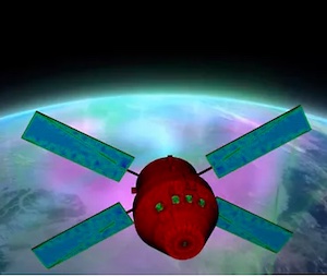
Aerospace, electronics and automotive industries must meet rigorous electrical performance requirements to mitigate safety risks related to charging and discharging events. Engineers need to be confident a spacecraft will survive exposure to space plasma. High-voltage systems must operate safely without risk of fire. Autonomous vehicles must maintain safety critical functions when faced with an unexpected electrical event. Without fully understanding and addressing these risks, companies may face costly late-phase redesigns, often totaling millions of dollars.
High-fidelity predictions from EMA3D Charge provide engineers with a deeper understanding of electrical charging and discharging phenomena. These insights can have a significant impact on product design, helping engineers determine how electrical components may be harmed — and to what extent — by charging and discharging events. Mitigating risks early in the design phase reduces the chances of late-stage redesigns and costly product failures.
“EMA3D Charge has an impressive array of capabilities,” said EMC engineers at NASA Johnson Space Center. “For example, its ability to easily manipulate and mesh mechanical computer-aided design (CAD) models greatly simplifies the process of going from a structural model of the spacecraft to analytical results. We have also seen great value in its ability to perform charging analysis on spacecraft that are being charged by direct contact with lunar dusts whilst simultaneously being charged from exposure to space plasmas on or near the lunar surface.”
While the technology within EMA3D Charge has been applied in the electronics and aerospace industry before, the solution is the first to be focused entirely on charging and discharging prediction. Leveraging Ansys SpaceClaim to create an intuitive user interface and workflow, EMA3D Charge combines CAD import, design and simplification, simulation setup and meshing, and result generalization and visualization into one solver technology.
“EMA3D Charge fills a need in a marketplace in which no other simulation product exists,” said Shane Emswiler, senior vice president of products at Ansys. “Engineers simulating charging and discharging events once had to navigate multiple codes and challenging workflows that fell short of a full solution. EMA3D Charge is a full solution—one that provides high-fidelity analysis and an end-to-end workflow designed for efficiency.”
Testimonial
"Our marketing partnership with I-Connect007 is already delivering. Just a day after our press release went live, we received a direct inquiry about our updated products!"
Rachael Temple - AlltematedSuggested Items
Global PCB Connections: Understanding the General Fabrication Process—A Designer’s Hidden Advantage
08/14/2025 | Markus Voeltz -- Column: Global PCB ConnectionsDesigners don’t need to become fabricators, but understanding the basics of PCB fabrication can save you time, money, and frustration. The more you understand what’s happening on the shop floor, the better you’ll be able to prevent downstream issues. As you move into more advanced designs like HDI, flex circuits, stacked vias, and embedded components, this foundational knowledge becomes even more critical. Remember: the fabricator is your partner.
The Art and Science of PCB Floor Planning: A Comprehensive Guide
08/14/2025 | Cory Grunwald and Jeff Reinhold, Monsoon SolutionsPCB design is an intricate and crucial part of developing electronic products. One of the foundational stages of PCB design is floor planning, a phase where the placement of components and the flow of signals are meticulously mapped out. A good floor plan ensures that the PCB performs well, is easy to manufacture, and meets all mechanical and electrical requirements. We’ll explore the essential aspects of floor planning, from its objectives and process to the challenges that designers face.
EnSilica Establishes New EU Mixed-Signal Design Centre in Budapest, Hungary
08/12/2025 | EnSilicaThe facility strengthens EnSilica’s presence in the European Union and taps into Budapest’s deep technology ecosystem, which hosts numerous leading automotive and industrial multinationals. This expansion will increase the Group’s global headcount to around 210 employees.
Happy’s Tech Talk #41: Sustainability and Circularity for Electronics Manufacturing
08/13/2025 | Happy Holden -- Column: Happy’s Tech TalkI attended INEMI’s June 12 online seminar, “Sustainable Electronics Tech Topic Series: PCBs and Sustainability.” Dr. Maarten Cauwe of imec spoke on “Life Cycle Inventory (LCI) Models for Assessing and Improving the Environmental Impact of PCB Assemblies,” and Jack Herring of Jiva Materials Ltd. spoke on “Transforming Electronics with Recyclable PCB Technology.” This column will review information and provide analysis from both presentations.
Elementary, Mr. Watson: Why Your PCB Looks Like a Studio Apartment
08/13/2025 | John Watson -- Column: Elementary, Mr. WatsonIn November 2022, I wrote a column called "Is Your Bathroom in the Kitchen?" This piece related a bizarre real estate listing that emerged out of St. Louis that had architects scratching their heads and interior designers cringing. Nestled in the historic Central West End sat a 200-square-foot apartment that completely defied logic. It wasn't the size that raised eyebrows, it was the layout. Here's the kicker: While that's rare in real estate, it's shockingly common in PCB design.