-

- News
- Books
Featured Books
- design007 Magazine
Latest Issues
Current Issue
Rules of Thumb
This month, we delve into rules of thumb—which ones work, which ones should be avoided. Rules of thumb are everywhere, but there may be hundreds of rules of thumb for PCB design. How do we separate the wheat from the chaff, so to speak?

Partial HDI
Our expert contributors provide a complete, detailed view of partial HDI this month. Most experienced PCB designers can start using this approach right away, but you need to know these tips, tricks and techniques first.

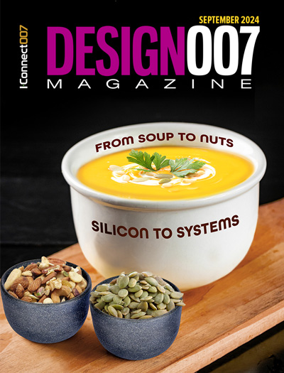
Silicon to Systems: From Soup to Nuts
This month, we asked our expert contributors to weigh in on silicon to systems—what it means to PCB designers and design engineers, EDA companies, and the rest of the PCB supply chain... from soup to nuts.
- Articles
- Columns
Search Console
- Links
- Media kit
||| MENU - design007 Magazine
Estimated reading time: 3 minutes
Contact Columnist Form
Trouble in Your Tank: Via Filling—Continued
Introduction
In a previous column, I presented several options with which to accomplish blind and through-hole via filling. In this edition of Trouble in Your Tank, filling blind vias and through-holes with polymeric pastes will be presented.
Via Fill Paste
Often the term “plugging paste” is used to describe the method and material of completely filling blind vias and through-holes. In general, paste filling material selection is at the request of the end user and is indicated for several reasons. It has been my experience that major OEMs are driving the industry to migrate to the high Tg/low CTE plugging paste formulations for high density applications. In addition, these formulations are of a non-conductive nature that provide a high quality plugged via, and are also cost effective (Figure 1). Limitations abound depending on PWB thickness, via diameter, and paste properties.
Properties of Via Fill Materials
What attributes are needed for a high performance via fill material? There are specific requirements for the plugging paste material. These are:
- Good adhesion between copper and paste, even under temperature influences
- Good adhesion of copper, dielectrics, or photoresist
- Solvent-free, one-pack system
- No air inclusions in the paste
- Tg > 140°C
- CTE < 40 ppm (below Tg)
- No shrinkage during curing
- Easily planarized
Additionally, the plugging paste material must maintain a reasonable shelf life at room temperature. Keep in mind that these materials are thermally reactive.
It is highly recommended that the fabricator uses a 100% solids content of the paste material with the thermally cross-linkable epoxy resin and specially designed ceramic fillers. The ceramic filling material restricts Z-axis expansion when the filled vias are subjected to a thermal load. Interestingly, the coefficient of thermal expansion must remain in the 40-60 ppm range to ensure that via cracks do not occur in the filled via. In addition, it is critical that Z-axis expansion be minimized to prevent the plated cap from lifting (Figure 2).
As noted previously, a properly formulated plugging paste for via fill must maintain a low CTE at and above 140?C. The ceramic particles that are formulated in the resin system function to restrain Z-axis expansion under thermal loading.
The ceramic fillers can be seen in Figure 3 under high magnification of the fully cured polymeric paste.
There is no disputing the fact that the vias must be filled void-free and maintain integrity throughout various thermal excursions. Z-axis expansion notwithstanding, the second critical thermal characteristic is the glass transition temperature of the cured paste material. Typically, a Tg of 140?C is ideal. However, the Tg can be increased by prolonging the final curing time and increasing curing temperature from 140?C to approximately 175-180?C. It is desired to have the highest possible Tg without impacting the flow and metallization properties1.
With increased densification leading to higher I/Os, smaller components, higher assembly temperatures, and smaller vias, the CTE gains increased importance. Thus, the CTE values of the paste must be minimized to relieve stress that will cause the plug to over expand, causing the over-metallized copper deposit to lift2. It is critical that to attain long term stability within the filled via under load conditions, load amplitudes must be minimized as much as possible. This means that the CTE must be as low as possible over the temperature ranges2.
Regardless of the method of via filling chosen, this is a process that is here to stay. Via filling technology is a critical aspect of HDI printed circuit board fabrication and the never-ending quest for miniaturization.
References
- Karsten Andra, “Hole Plugging Technology for Multilayers and HDI Packages,” EPC PCB Convention, 1999.
- Internal communication with Lackwerke Peters.
This column originally appeared in the October 2021 issue of PCB007 Magazine.
More Columns from Trouble in Your Tank
Trouble in Your Tank: Interconnect Defect—The Three Degrees of SeparationTrouble in Your Tank: Things You Can Do for Better Wet Process Control
Trouble in Your Tank: Processes to Support IC Substrates and Advanced Packaging, Part 5
Trouble in Your Tank: Materials for PWB Fabrication—Drillability and Metallization
Trouble in Your Tank: Supporting IC Substrates and Advanced Packaging, Part 5
Trouble in Your Tank: Electrodeposition of Copper, Part 6
Trouble in Your Tank: Electrolytic Copper Plating, Part 5
Trouble in Your Tank: Processes to Support IC Substrates and Advanced Packaging, Part 4


