-
- News
- Books
Featured Books
- pcb007 Magazine
Latest Issues
Current IssueThe Hole Truth: Via Integrity in an HDI World
From the drilled hole to registration across multiple sequential lamination cycles, to the quality of your copper plating, via reliability in an HDI world is becoming an ever-greater challenge. This month we look at “The Hole Truth,” from creating the “perfect” via to how you can assure via quality and reliability, the first time, every time.
In Pursuit of Perfection: Defect Reduction
For bare PCB board fabrication, defect reduction is a critical aspect of a company's bottom line profitability. In this issue, we examine how imaging, etching, and plating processes can provide information and insight into reducing defects and increasing yields.
Voices of the Industry
We take the pulse of the PCB industry by sharing insights from leading fabricators and suppliers in this month's issue. We've gathered their thoughts on the new U.S. administration, spending, the war in Ukraine, and their most pressing needs. It’s an eye-opening and enlightening look behind the curtain.
- Articles
- Columns
- Links
- Media kit
||| MENU - pcb007 Magazine
American Standard Circuits Utilizes Averatek Process for Medical Technology
December 6, 2021 | American Standard CircuitsEstimated reading time: 1 minute

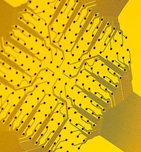
Mr. Anaya Vardya, President and CEO of American Standard Circuits recently discussed how using the Averatek A-SAP™ process allows his company to better service their medical electronics customers.
When commenting on this process Mr. Vardya explained, “Our medical electronics customers depend on us to provide them with the most reliable PCBs possible. When dealing with medical products it is not hyperbole to say that it is always a matter of life or death. With the A-SAP™ manufacturing process ASC can now provide our customers with ultra high-density technology, 25 micron trace and space, and improved reliability, reducing layer counts and micro via lamination cycles, ultimately simplifying the design. Other advantages include improved signal intergrity, aspect ratios greater than 1:1 for metal traces and extremely tight tolerances. Specific to medical technology, this process is not limited to copper conductors and enables the use of gold as a conductive metal to deliver bio-compatibility advantages. In many instances the reduced layer count allows for improved costs which we then pass on to our medical customers. It’s a win-win situation for both of us.”
Visit I-007eBooks to download your copies of American Standard Circuits’ micro eBooks today:
The Printed Circuit Designer’s Guide to... Fundamentals of RF/ Microwave PCBs
The Printed Circuit Designer's Guide to... Flex and Rigid-Flex Fundamentals
The Printed Circuit Designer’s Guide to... Thermal Management: A Fabricator’s Perspective
And be sure to check out Realtime with... American Standard Circuits to learn more!
About American Standard Circuits
American Standard Circuits (ASC) prides itself on being a total solutions provider, manufacturing quality rigid, metal-backed, RF/microwave, flex, and rigid-flex PCBs for the medical, automotive, industrial, defense, and aerospace markets in volumes from test and prototypes to large production orders. ASC has the expertise to provide a wide variety of technologies in a time-critical environment. Their qualifications include AS9100 Rev D, ISO 9001:2015, MIL-PRF 31032, MIL-PRF-55110, MIL-PRF-50884 certification and ITAR registration. In addition to manufacturing in the USA, ASC can transition and manage your PCB requirements to lower cost regions via its qualified supply chain of offshore partners. ASC also holds many key patents for metal bonding processes. For more information about American Standard Circuits' services or to ask one of their technology experts a question go to www.asc-i.com.
Suggested Items
The Evolution of Picosecond Laser Drilling
06/19/2025 | Marcy LaRont, PCB007 MagazineIs it hard to imagine a single laser pulse reduced not only from nanoseconds to picoseconds in its pulse duration, but even to femtoseconds? Well, buckle up because it seems we are there. In this interview, Dr. Stefan Rung, technical director of laser machines at Schmoll Maschinen GmbH, traces the technology trajectory of the laser drill from the CO2 laser to cutting-edge picosecond and hybrid laser drilling systems, highlighting the benefits and limitations of each method, and demonstrating how laser innovations are shaping the future of PCB fabrication.
Day 2: More Cutting-edge Insights at the EIPC Summer Conference
06/18/2025 | Pete Starkey, I-Connect007The European Institute for the PCB Community (EIPC) summer conference took place this year in Edinburgh, Scotland, June 3-4. This is the third of three articles on the conference. The other two cover Day 1’s sessions and the opening keynote speech. Below is a recap of the second day’s sessions.
Day 1: Cutting Edge Insights at the EIPC Summer Conference
06/17/2025 | Pete Starkey, I-Connect007The European Institute for the PCB Community (EIPC) Summer Conference took place this year in Edinburgh, Scotland, June 3-4. This is the second of three articles on the conference. The other two cover the keynote speeches and Day 2 of the technical conference. Below is a recap of the first day’s sessions.
Preventing Surface Prep Defects and Ensuring Reliability
06/10/2025 | Marcy LaRont, PCB007 MagazineIn printed circuit board (PCB) fabrication, surface preparation is a critical process that ensures strong adhesion, reliable plating, and long-term product performance. Without proper surface treatment, manufacturers may encounter defects such as delamination, poor solder mask adhesion, and plating failures. This article examines key surface preparation techniques, common defects resulting from improper processes, and real-world case studies that illustrate best practices.
RF PCB Design Tips and Tricks
05/08/2025 | Cherie Litson, EPTAC MIT CID/CID+There are many great books, videos, and information online about designing PCBs for RF circuits. A few of my favorite RF sources are Hans Rosenberg, Stephen Chavez, and Rick Hartley, but there are many more. These PCB design engineers have a very good perspective on what it takes to take an RF design from schematic concept to PCB layout.