-
- News
- Books
Featured Books
- design007 Magazine
Latest Issues
Current IssueProper Floor Planning
Floor planning decisions can make or break performance, manufacturability, and timelines. This month’s contributors weigh in with their best practices for proper floor planning and specific strategies to get it right.
Showing Some Constraint
A strong design constraint strategy carefully balances a wide range of electrical and manufacturing trade-offs. This month, we explore the key requirements, common challenges, and best practices behind building an effective constraint strategy.
All About That Route
Most designers favor manual routing, but today's interactive autorouters may be changing designers' minds by allowing users more direct control. In this issue, our expert contributors discuss a variety of manual and autorouting strategies.
- Articles
- Columns
- Links
- Media kit
||| MENU - design007 Magazine
Pulsonix PCB Design Adds 3D Collision Detection for Multi-board and Board Folding in Version 12.0
April 13, 2022 | PulsonixEstimated reading time: 2 minutes

Pulsonix, the Electronic Design Automation (EDA) company delivering technology-leading PCB design solutions, announced the release of Pulsonix version 12.0, which adds new capabilities, significant speed improvements, and highly requested usability enhancements.
“Version 12.0 offers a significant step up for our users in the areas of the PCB design process that they say would benefit them the most, ” said Bob Williams, marketing director for Pulsonix. “The new 3D design features along with 64-bit processing and multi-core support allow our designers to quickly visualize design changes in 3D even with large designs and stacked boards.”
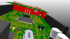
Pulsonix 3D capabilities now include 3D collision detection for both multi-board designs and board folding. This allows designers to visualize boards in a stacked or folded configuration and to verify boards and components fit together in the intended space. Automated clash detection will flag any space violations, and there is a new capability that allows designers to ignore clashes that are intended for known connection points like plugs and sockets.
These new 3D capabilities are integrated into a new consolidated 3D design menu that organizes setup and operation for a more intuitive workflow. This simplifies the interface and enables new functionality while minimizing complexity.
Pulsonix 12.0 is significantly faster due to the new 64-bit implementation and additional multi-threading capabilities to speed up time-consuming functions. Two specific examples are 1) users with large designs will see significant speed ups due to the increased 64-bit address space and multi-threading for library access, and 2) 3D rendering is now multi-threaded meaning 3D viewing and STEP output can be spread across multiple cores and completed in less than half the time.
“Another common request is Dark Mode for the user interface,” added Williams. “Not only does the new Dark Mode option change to a dark background scheme, but we also swap out all toolbar icons to a set that is more compatible with Dark Mode. Whether it's for less eye strain, lower power consumption, or just aesthetics, I'm sure Dark Mode will be a popular feature.”
Additional Rules and DRC checking add new functionality to the Interactive High-Speed option. With new rules such as stub routing length, loop antenna, return path, SMD to corner, and SMD to plane rules, more precision when designing critical advanced circuits can be achieved. Additional enhancements to the editing of differential pair tracks further endorse the precision of Pulsonix.
“With almost 100 documentable additions and changes, Pulsonix Version 12.0 is a significant release with advanced technology and features that directly benefit our customers,” added Williams.
Testimonial
"In a year when every marketing dollar mattered, I chose to keep I-Connect007 in our 2025 plan. Their commitment to high-quality, insightful content aligns with Koh Young’s values and helps readers navigate a changing industry. "
Brent Fischthal - Koh YoungSuggested Items
Global PCB Connections: Understanding the General Fabrication Process—A Designer’s Hidden Advantage
08/14/2025 | Markus Voeltz -- Column: Global PCB ConnectionsDesigners don’t need to become fabricators, but understanding the basics of PCB fabrication can save you time, money, and frustration. The more you understand what’s happening on the shop floor, the better you’ll be able to prevent downstream issues. As you move into more advanced designs like HDI, flex circuits, stacked vias, and embedded components, this foundational knowledge becomes even more critical. Remember: the fabricator is your partner.
The Art and Science of PCB Floor Planning: A Comprehensive Guide
08/14/2025 | Cory Grunwald and Jeff Reinhold, Monsoon SolutionsPCB design is an intricate and crucial part of developing electronic products. One of the foundational stages of PCB design is floor planning, a phase where the placement of components and the flow of signals are meticulously mapped out. A good floor plan ensures that the PCB performs well, is easy to manufacture, and meets all mechanical and electrical requirements. We’ll explore the essential aspects of floor planning, from its objectives and process to the challenges that designers face.
EnSilica Establishes New EU Mixed-Signal Design Centre in Budapest, Hungary
08/12/2025 | EnSilicaThe facility strengthens EnSilica’s presence in the European Union and taps into Budapest’s deep technology ecosystem, which hosts numerous leading automotive and industrial multinationals. This expansion will increase the Group’s global headcount to around 210 employees.
Happy’s Tech Talk #41: Sustainability and Circularity for Electronics Manufacturing
08/13/2025 | Happy Holden -- Column: Happy’s Tech TalkI attended INEMI’s June 12 online seminar, “Sustainable Electronics Tech Topic Series: PCBs and Sustainability.” Dr. Maarten Cauwe of imec spoke on “Life Cycle Inventory (LCI) Models for Assessing and Improving the Environmental Impact of PCB Assemblies,” and Jack Herring of Jiva Materials Ltd. spoke on “Transforming Electronics with Recyclable PCB Technology.” This column will review information and provide analysis from both presentations.
Elementary, Mr. Watson: Why Your PCB Looks Like a Studio Apartment
08/13/2025 | John Watson -- Column: Elementary, Mr. WatsonIn November 2022, I wrote a column called "Is Your Bathroom in the Kitchen?" This piece related a bizarre real estate listing that emerged out of St. Louis that had architects scratching their heads and interior designers cringing. Nestled in the historic Central West End sat a 200-square-foot apartment that completely defied logic. It wasn't the size that raised eyebrows, it was the layout. Here's the kicker: While that's rare in real estate, it's shockingly common in PCB design.