


 The Chemical Connection: Through-glass Vias in Glass Substrates
 It’s Only Common Sense: Why Sales Teams Fail (and How to Fix Them)
 The Marketing Minute: A Brand Visibility Playbook—Get Seen, Heard, and Remembered


Indium Corporation Introduces New Cleanable SiPaste for Fine Feature Printing
December 28, 2022 | Indium CorporationEstimated reading time: Less than a minute
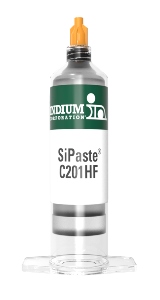
Indium Corporation has added to its portfolio of pastes for fine feature printing with a halogen-free, cleanable solder paste specifically formulated to accommodate fine feature printing, as seen with 01005 and 008004 components.
SiPaste C201HF combines superior, industry-leading non-wet open (NWO) performance with excellent stencil print transfer efficiency to satisfy the broadest range of process requirements and boost SPI yields. It leaves behind a cleanable residue, able to be removed with a commercially available semi-aqueous cleaning solution, or it can be used as a standard no-clean paste in processes where post-reflow cleaning is not applicable.
SiPaste C201HF features excellent transfer efficiency on fine feature apertures, with consistent process yields below 80?m. SiPaste® C201HF delivers:
- Consistent and tight solder deposit spread across multiple prints; excellent response-to-pause performance
- Minimal voiding on tight-pitch components, ensuring joint strength on small components
- Excellent reflow performance on components that exhibit high warpage
- Enhanced slump performance with minimal bridging during the assembly process, improving yields for tight-pitch components
- Flexible cleaning; can be used in processes that require cleaning with a saponifier or that do not require cleaning
Share on:


Suggested Items
SolderKing’s Successful Approach to Modern Soldering Needs
06/18/2025 | Nolan Johnson, I-Connect007Chris Ward, co-founder of the family-owned SolderKing, discusses his company's rapid growth and recent recognition with the King’s Award for Enterprise. Chris shares how SolderKing has achieved these award-winning levels of service in such a short timeframe. Their secret? Being flexible in a changing market, technical prowess, and strong customer support.
Preventing Surface Prep Defects and Ensuring Reliability
06/10/2025 | Marcy LaRont, PCB007 MagazineIn printed circuit board (PCB) fabrication, surface preparation is a critical process that ensures strong adhesion, reliable plating, and long-term product performance. Without proper surface treatment, manufacturers may encounter defects such as delamination, poor solder mask adhesion, and plating failures. This article examines key surface preparation techniques, common defects resulting from improper processes, and real-world case studies that illustrate best practices.
Breaking Silos with Intelligence: Connectivity of Component-level Data Across the SMT Line
06/09/2025 | Dr. Eyal Weiss, CybordAs the complexity and demands of electronics manufacturing continue to rise, the smart factory is no longer a distant vision; it has become a necessity. While machine connectivity and line-level data integration have gained traction in recent years, one of the most overlooked opportunities lies in the component itself. Specifically, in the data captured just milliseconds before a component is placed onto the PCB, which often goes unexamined and is permanently lost once reflow begins.
BEST Inc. Introduces StikNPeel Rework Stencil for Fast, Simple and Reliable Solder Paste Printing
06/02/2025 | BEST Inc.BEST Inc., a leader in electronic component rework services, training, and products is pleased to introduce StikNPeel™ rework stencils. This innovative product is designed for printing solder paste for placement of gull wing devices such as quad flat packs (QFPs) or bottom terminated components.
See TopLine’s Next Gen Braided Solder Column Technology at SPACE TECH EXPO 2025
05/28/2025 | TopLineAerospace and Defense applications in demanding environments have a solution now in TopLine’s Braided Solder Columns, which can withstand the rigors of deep space cold and cryogenic environments.