


 Fresh PCB Concepts: Engineering Copper Coin and Copper Pedestal Technology With IPC Design Interpretation
 Target Condition: Signal Integrity Without Borders
 Elementary, Mr. Watson: PCB Education in the Midst of the Storms


Keysight Technologies, Inc., a leading technology company that delivers advanced design and validation solutions to help accelerate innovation to connect and secure the world, introduces the Electrical Performance Scan (EP-Scan), a new high-speed digital simulation tool that supports rapid signal integrity (SI) analysis for hardware engineers and printed circuit board (PCB) designers.
After completing a PCB design, hardware engineers hand the design over to SI specialists to validate its performance before going to prototype. SI specialists perform simulations on a large number of nets, which can take days to weeks to complete. As a result, hardware engineers have difficulty predicting how much analysis time it will take to find errors or performance issues in the design. Uncertainty about the length of the SI analysis phase creates a bottleneck in the design cycle and delays time-to-market.
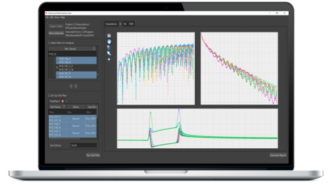
EP-Scan addresses SI analysis bottlenecks by giving hardware designers diagnostic tools to correct designs earlier and meet development schedules. As a stand-alone software product, EP-Scan performs electromagnetic (EM) simulation on signal nets and reports SI metrics such as channel return and insertion loss. In addition, EP-Scan automates performance comparisons between different versions of a design and generates simulation reports that expedite verification prior to building expensive physical prototypes.
"Our goal with EP-Scan is to 'shift left' the PCB design verification process by using early simulation to detect and correct errors, giving hardware designers the confidence to move forward and obtain first pass success," said Tim Wang-Lee, Ph.D., Product Marketing Manager at Keysight. "I am proud that EP-Scan is helping engineers to spend more time doing analyses to gain insights, documenting results to track progress, and automating routine tests. EP-Scan empowers hardware engineers by maximizing their productivity."
EP-Scan requires only the layout geometry and substrate stack-up information for the PCB design as inputs. After engineers specify the desired nets for investigation, EP-Scan reports simulation results including the characteristic impedance and delay of traces, return loss, insertion loss, and impedance time-domain reflectometry (TDR). By analyzing common fabrication formats such as ODB++, EP-Scan shows engineers the performance of their design as it would be when fabricated. EP-Scan enables hardware engineers to quickly validate designs and identify layout issues before the final verification, which reduces time-to-market, and can contribute to more PCB design wins.


