-

- News
- Books
Featured Books
- design007 Magazine
Latest Issues
Current Issue
Designing Through the Noise
Our experts discuss the constantly evolving world of RF design, including the many tradeoffs, material considerations, and design tips and techniques that designers and design engineers need to know to succeed in this high-frequency realm.

Learning to Speak ‘Fab’
Our expert contributors clear up many of the miscommunication problems between PCB designers and their fab and assembly stakeholders. As you will see, a little extra planning early in the design cycle can go a long way toward maintaining open lines of communication with the fab and assembly folks.

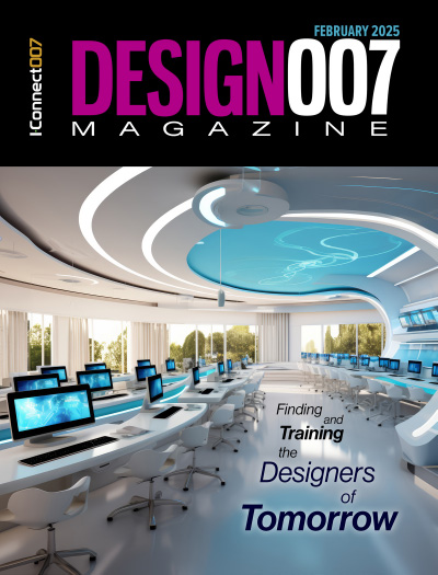
Training New Designers
Where will we find the next generation of PCB designers and design engineers? Once we locate them, how will we train and educate them? What will PCB designers of the future need to master to deal with tomorrow’s technology?
- Articles
- Columns
Search Console
- Links
- Media kit
||| MENU - design007 Magazine
Book Excerpt: 'The Printed Circuit Designer's Guide to... Manufacturing Driven Design,' Chapter 5
September 20, 2023 | I-Connect007 Editorial TeamEstimated reading time: 2 minutes
Excerpt from: The Printed Circuit Designer's Guide to... Manufacturing Driven Design, Chapter 5: Using the Cloud to Accelerate New Product Introductions
Improving Upon Reliability
The importance of validating that a design can be produced with yield, cost, and reliability in mind is important to a successful product launch. This is regardless of whether its manufacturability is ensured based on the traditional DFM approach, or through the Manufacturing Driven Design approach suggested here.
The electronics produced today are more relied upon than ever before. Many historians point to this adoption beginning with the space race. In 1977, twin space probes, Voyager 1 and 2, were launched. To ensure reliability, the deep space probe was built with dual-redundancy on every computerized system—two Computer Command Systems (CCS), two Flight Data Systems (FDS), and dual Attitude Articulation Control Systems (AACS). Even the two computer command systems were built with dual redundancy, two power supplies, two processors, and two buffers; these could operate independently, in parallel, or in tandem with one another.5 Their intended mission length was five years. Forty-five years later that technology is still sending bits of data back to Earth from interstellar space.
Today’s electronics respond fast enough to enable rockets to propel a payload into space, return autonomously, and safely land, completing a process that human reflexes could never be fast enough to do alone. Back on Earth, untold thousands count on medical implants to keep us alive. A higher level of importance on the reliability of electronics is closer to all of us and that dependance is ever increasing. If you doubt that, just try to take a mobile phone from a teenager and see how that goes.
To improve upon reliability, all PCB manufacturers are ready and prepared to participate in the planning for PCB production right at the start of the design stage. Most manufacturers suggest that following general guidelines would at the very least minimize manufacturing problems and at the very best reduce cost. Using MDD, the manufacturing process capabilities become defined and shared by PCB manufacturers in a modern collaborative fashion. With this model there is no need for traditional documentation, as there is no longer a need for the designers to understand and interpret all the manufacturer’s capabilities. Design organizations often lack the required manufacturing knowledge and find manufacturing topics often unclear, missing important aspects, and even more important to the manufacturer, quickly out of date.
If 45 years after the launch of Voyager 1, documentation is still how manufacturing capabilities are communicated into design, the industry should take a deep look and evaluate how innovation today would result in a brighter future tomorrow. Innovation begins with overcoming limitations imposed by restricting the use of information, and moving toward the idea of forward thinking, where such sharing is to the mutual benefit of both parties.
Visit I-007eBooks to continue reading this book.
Suggested Items
IDTechEx Highlights Recyclable Materials for PCBs
04/10/2025 | IDTechExConventional printed circuit board (PCB) manufacturing is wasteful, harmful to the environment and energy intensive. This can be mitigated by the implementation of new recyclable materials and technologies, which have the potential to revolutionize electronics manufacturing.
Incap US Invests in Advanced SMT Technology
04/09/2025 | IncapIncap Electronics US invested approximately USD 2 million (EUR 1.82 million) in advanced SMT (surface-mount technology) production equipment to expand its production capacity.
Cirtronics to Lead Robotics Commercialization Discussion at 2025 Robotics Summit & Expo
04/09/2025 | CirtronicsCirtronics, a leading contract manufacturer specializing in complex robotics builds, will host a must-attend panel discussion at the Robotics Summit & Expo, April 30 – May 1 at the Boston Convention & Exhibition Center.
Siemens Acquires DownStream Technologies to Expand PCB Design-to-Manufacturing Flow
04/08/2025 | SiemensSiemens Digital Industries Software announced that it has completed the acquisition of DownStream Technologies, a leading provider of manufacturing data preparation solutions for printed circuit board (PCB) design.
Nano Dimension Appoints Ofir Baharav as CEO
04/08/2025 | Nano DimensionNano Dimension Ltd., a digital manufacturing leader, announced the appointment of Mr. Ofir Baharav as its new Chief Executive Officer, effective immediately.


