


 It’s Only Common Sense: Creativity Is Noisy, Messy, and So Worth It
 Dan’s Biz Bookshelf: ‘The Soul of a New Machine’


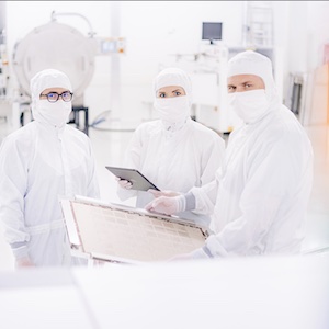
AT&S quickly established itself as a reliable substrate supplier for AMD and is currently preparing a significant expansion of capacity for AMD. “AMD’s quality requirements are very high, which makes us very proud to have achieved the ramp-up so fast. Currently, we are preparing facilities at our new plant in Kulim, Malaysia, to expand our AMD capacity,” says AT&S CEO Andreas Gerstenmayer. The demand for CPUs and GPUs for datacenters is expected to continue growing healthily in the next couple of years, which will help to strengthen the partnership between AMD and AT&S: “Fueled by new technologies like AI, VR and AR, demand for data storage, transmission and analysis is rising globally,” says Gerstenmayer.
To meet the accelerating demand for powerful and sustainable computing, AMD is pushing the boundaries of innovation in chip design as well as packaging to deliver faster and more energy efficient chips. “AT&S can provide a lot of know-how in this field. We are already working on new technologies for substrates that will allow our customers to integrate a high number of chips into very fast and efficient packaged systems that will help to analyze and transmit data in the cloud fast and reliably,” says AT&S Executive Vice President of Business Unit Micro Electronics, Ingolf Schröder.
“The last few years have demonstrated the critical role that semiconductors play in enabling our world and have shown us the importance of having a strong and geographically diverse supply chain,” says Keivan Keshvari, AMD Senior Vice President of Global Operations. “At AMD, we collaborate closely with all of our suppliers to enhance business continuity plans. We are pleased to have found an innovative and reliable additional source for high-end substrates in AT&S and look forward to leveraging the new site to deliver high-performance and adaptive computing products that drive continued growth in the data center and AI markets.”
Future Market “Advanced Packaging”
AT&S is one of the leaders for embedding microchips and components that regulate the associated power and information flows into monolithic systems that make sure that the pathways stay as short as possible, so information can travel at maximum speed without any significant losses. The big substrates that are necessary to build such integrated systems are optimized for reliability and efficiency by using AT&S’s sophisticated simulation technology. “We are among the technology leaders in the substrate market and have an additional advantage because we can offer manufacturing capacity not only in China but also in Malaysia and Austria,” says AT&S CEO Gerstenmayer.


