


 Beyond Design: Termination Planning
 Elementary, Mr. Watson: Cultivating a Culture of Collaboration
 Connect the Dots: Designing for Reality—Lamination and Materials
Koh Young at SEMICON West with a Focus on Inspection & Metrology for Semiconductor and Advanced Packaging Challenges
June 4, 2024 | Koh YoungEstimated reading time: 1 minute
Koh Young, the industry leader in True3D measurement-based inspection solutions, will demonstrate its ZenStar and Meister Series of automated inspection and metrology tools for semiconductor and advanced package applications in booth 1833 at SEMICON West, taking place from July 9-11, 2024, at the Moscone Center in San Francisco, CA.
For over two decades, Koh Young has been a global leader in the field of 3D inspection and measurement technology. Our journey began with a vision to enhance precision and efficiency in electronics manufacturing. Today, we stand at the forefront of revolutionizing the semiconductor industry with our innovative metrology solutions. Using our True3D™ measurement-based inspection technologies, including the ZenStar and Meister Series, manufacturers can tackle critical manufacturing challenges in advanced packaging. These technologies provide real-time insights and predictive analytics to drive smarter manufacturing decisions, achieve higher yields, reduce defects, and improve overall productivity.
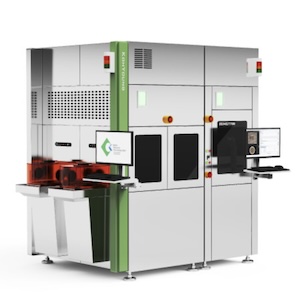
Meister S Premium In-line 3D Inspection System for Micro Solder Paste Deposits
Combining innovative vision algorithms and high-resolution optic technology, the Meister S is the ultimate, True 3D SPI solution for the semiconductor & Mini/Micro-LED packaging process improvement.
- High-resolution optics with a high-speed camera system (0.1 µm Z resolution)
- High-speed 25 Mega-pixel Camera with 3.5-micron Resolution Optics
- 10-micron Thins Solder Paste Inspection
- Colored and Transparent Flux Inspection
Meister D+ Breakthrough in 3D Measurement for Highly Reflective, Shiny Die
The Meister D+ combines industry-leading Moiré technology to inspect for micro cracks, chipping, foreign material, and more and our new proprietary optics to support highly-reflective die inspection, a challenge historically plaguing the industry.
- Small Die and Component Inspection (0201 metric / 008004 EIA)
- Narrow-gap Inspection down to 50-microns
- Height and Tilt Measurement in High Density, Highly Reflective Applications
ZenStar True 3D Measurement for Wafer-level Packaging Applications
Combining innovative vision algorithms and high-resolution optical technology, the ZenStar inspects highly reflective die as well as components. With proprietary deep learning technology, it offers enhanced capabilities to inspect defects like micro-cracks, foreign material, chipping, and more.
- Industry-leading metrology capabilities with deep learning technology
- 10-micron diameter wafer bump inspection
- Full 3D height and tilt measurement for even highly reflective die surfaces
Share on:


Suggested Items
ViTrox Americas Opens New State-of-the-Art Demo Lab in Hutto, Texas
06/27/2024 | ViTroxViTrox Americas Inc. is proud to announce the opening of its new demo lab in Hutto, Texas. This cutting-edge facility is now ready for demonstrations and evaluations, showcasing ViTrox's latest innovations in 3D inspection technology.
TRI Expands with New Office in Guadalajara, Mexico
06/19/2024 | TRITest Research, Inc. (TRI), the leading Test and Inspection systems provider for the electronics manufacturing industry, recently opened a new office in Guadalajara, Mexico, to accommodate the industry's rapid growth.
Zero Defects International to Exhibit At SMTA Oregon Expo
06/19/2024 | Zero Defects InternationalZero Defects International [ZDI] has announced their participation as an exhibitor at the SMTA Expo and Tech Forum to be held Thursday, June 20 at the Wingspan Event & Conference Center in Hillsboro, Oregon. Location of this venue is 801 NE 34th Ave., Hillsboro, Oregon.
Standard of Excellence: Looking Five Years Into the Future
06/19/2024 | Anaya Vardya -- Column: Standard of ExcellenceThe future of the PCB industry will be based on technology. As components get smaller, denser, and more complicated, PCB fabrication companies must keep up with their customers’ needs both today and in the future. It is no longer enough to just keep up with our customers’ current needs. We must be prepared to meet their PCB needs three to five years out. We need a complete understanding of where our customers are going and what they will need in the near distant future.
TRI to Drive AI Innovation in Smart Factories, in Collaboration with NVIDIA
06/03/2024 | TRITest Research, Inc., the leading test and inspection systems provider for the electronics manufacturing industry, announced a collaboration with NVIDIA and leading Taiwanese electronics manufacturers to accelerate the deployment of AI-driven technologies for smart factories.