-
- News
- Books
Featured Books
- smt007 Magazine
Latest Issues
Current Issue
Production Software Integration
EMS companies need advanced software systems to thrive and compete. But these systems require significant effort to integrate and deploy. What is the reality, and how can we make it easier for everyone?
Spotlight on India
We invite you on a virtual tour of India’s thriving ecosystem, guided by the Global Electronics Association’s India office staff, who share their insights into the region’s growth and opportunities.
Supply Chain Strategies
A successful brand is built on strong customer relationships—anchored by a well-orchestrated supply chain at its core. This month, we look at how managing your supply chain directly influences customer perception.
- Articles
- Columns
- Links
- Media kit
||| MENU - smt007 Magazine
Koh Young at SEMICON West with a Focus on Inspection & Metrology for Semiconductor and Advanced Packaging Challenges
June 4, 2024 | Koh YoungEstimated reading time: 1 minute
Koh Young, the industry leader in True3D measurement-based inspection solutions, will demonstrate its ZenStar and Meister Series of automated inspection and metrology tools for semiconductor and advanced package applications in booth 1833 at SEMICON West, taking place from July 9-11, 2024, at the Moscone Center in San Francisco, CA.
For over two decades, Koh Young has been a global leader in the field of 3D inspection and measurement technology. Our journey began with a vision to enhance precision and efficiency in electronics manufacturing. Today, we stand at the forefront of revolutionizing the semiconductor industry with our innovative metrology solutions. Using our True3D™ measurement-based inspection technologies, including the ZenStar and Meister Series, manufacturers can tackle critical manufacturing challenges in advanced packaging. These technologies provide real-time insights and predictive analytics to drive smarter manufacturing decisions, achieve higher yields, reduce defects, and improve overall productivity.
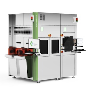
Meister S Premium In-line 3D Inspection System for Micro Solder Paste Deposits
Combining innovative vision algorithms and high-resolution optic technology, the Meister S is the ultimate, True 3D SPI solution for the semiconductor & Mini/Micro-LED packaging process improvement.
- High-resolution optics with a high-speed camera system (0.1 µm Z resolution)
- High-speed 25 Mega-pixel Camera with 3.5-micron Resolution Optics
- 10-micron Thins Solder Paste Inspection
- Colored and Transparent Flux Inspection
Meister D+ Breakthrough in 3D Measurement for Highly Reflective, Shiny Die
The Meister D+ combines industry-leading Moiré technology to inspect for micro cracks, chipping, foreign material, and more and our new proprietary optics to support highly-reflective die inspection, a challenge historically plaguing the industry.
- Small Die and Component Inspection (0201 metric / 008004 EIA)
- Narrow-gap Inspection down to 50-microns
- Height and Tilt Measurement in High Density, Highly Reflective Applications
ZenStar True 3D Measurement for Wafer-level Packaging Applications
Combining innovative vision algorithms and high-resolution optical technology, the ZenStar inspects highly reflective die as well as components. With proprietary deep learning technology, it offers enhanced capabilities to inspect defects like micro-cracks, foreign material, chipping, and more.
- Industry-leading metrology capabilities with deep learning technology
- 10-micron diameter wafer bump inspection
- Full 3D height and tilt measurement for even highly reflective die surfaces
Testimonial
"Your magazines are a great platform for people to exchange knowledge. Thank you for the work that you do."
Simon Khesin - Schmoll MaschinenSuggested Items
New Episode of Voices of the Industry Podcast Explores Breakthroughs in Test and Inspection
10/22/2025 | I-Connect007In this episode of Voices of the Industry, “Testing Innovation: Advances in Test, Inspection & Failure Analysis,” host Nolan Johnson speaks with Rob Boguski, president of Datest. Together, they explore the expanding world of circuit testing, inspection, and failure analysis, areas that are experiencing a surge in technological capability and sophistication. As Johnson and Boguski discuss, today’s test companies are performing analyses and precision methods that would have seemed impossible just a decade ago.
Knocking Down the Bone Pile: Revamp Your Components with BGA Reballing
10/14/2025 | Nash Bell -- Column: Knocking Down the Bone PileBall grid array (BGA) components evolved from pin grid array (PGA) devices, carrying over many of the same electrical benefits while introducing a more compact and efficient interconnect format. Instead of discrete leads, BGAs rely on solder balls on the underside of the package to connect to the PCB. In some advanced designs, solder balls are on both the PCB and the BGA package. In stacked configurations, such as package-on-package (PoP), these solder balls also interconnect multiple packages, enabling higher functionality in a smaller footprint.
Koh Young Discussing Ways to Apply Smart Factory Insights to Maximizing Productivity at SMTA Tijuana
10/14/2025 | Koh YoungKoh Young, the industry leader in True 3D measurement-based inspection solutions, will present at the SMTA Tijuana Expo & Tech Forum on November 13, 2025, at the Quartz Hotel in Tijuana, Baja California.
The Training Connection, LLC Welcomes Industry Veteran Jack Harris to Lead Training Partnerships
10/07/2025 | The Training Connection LLCThe Training Connection, LLC (TTC-LLC), a premier provider of test engineering and development training, is proud to announce that Jack Harris, one of the most recognized names in electronics manufacturing training and technical development, has joined the company as Relationship Lead, Training.
Now Available—The Companion Guide to… SMT Inspection: Today, Tomorrow, and Beyond: Mastering Metrology for Advanced Semiconductor Packages
10/03/2025 | I-Connect007I-Connect007 is pleased to announce the release of an 18-page resource for engineers, technologists, and decision-makers in electronics manufacturing: The Companion Guide to SMT Inspection: Today, Tomorrow, and Beyond: Mastering Metrology for Advanced Semiconductor Packages.