-

- News
- Books
Featured Books
- smt007 Magazine
Latest Issues
Current Issue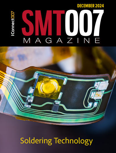
Soldering Technologies
Soldering is the heartbeat of assembly, and new developments are taking place to match the rest of the innovation in electronics. There are tried-and-true technologies for soldering. But new challenges in packaging, materials, and sustainability may be putting this key step in flux.
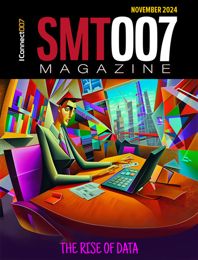
The Rise of Data
Analytics is a given in this industry, but the threshold is changing. If you think you're too small to invest in analytics, you may need to reconsider. So how do you do analytics better? What are the new tools, and how do you get started?
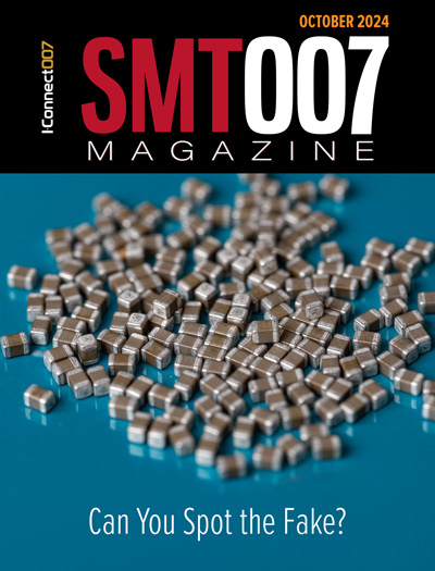
Counterfeit Concerns
The distribution of counterfeit parts has become much more sophisticated in the past decade, and there's no reason to believe that trend is going to be stopping any time soon. What might crop up in the near future?
- Articles
- Columns
Search Console
- Links
- Media kit
||| MENU - smt007 Magazine
Silicon Box Selects Piedmont to Host €3.2B Chip Foundry for Italian Expansion
July 2, 2024 | Silicon BoxEstimated reading time: 3 minutes
The co-founders of Silicon Box, CEO Dr. Byung Joon (BJ) Han, Dr. Sehat Sutardja, and Weili Dai, together with the Minister Adolfo Urso, Presidente Alberto Cirio of the Piedmont region, and Mayor Alessandro Canelli of the municipality of Novara announced that Novara in Piedmont will be the site of the company’s new, first-of-a-kind advanced semiconductor packaging and testing foundry. The parties signed a letter of intent outlining their commitment for collaboration related to the site and investment, this morning, at the Ministry of Enterprises and Made in Italy in Rome, subject to the European Commission approval of the planned financial support to be granted by Italy.
The site in Novara and Piedmont was selected from a shortlist of sites and regions in Northern Italy (Nord Italia) through a detailed evaluation process. This effort aimed at ensuring that selection be aligned with the requirements and conditions necessary for the planned facility, and prior commitments agreed between Silicon Box and the Italian government.
“Silicon Box’s advanced packaging facility in Novara is expected to create up to 1,600 highly paid jobs and bring first-of-a-kind advanced semiconductor packaging and testing capabilities to Italy, and to Europe,” said Dr. Byung Joon Han, CEO and cofounder of Silicon Box. “We appreciate the cooperation of all the sites, municipalities and regions that participated in our evaluation process. Every site was carefully reviewed and considered, and each had its own independent merits that reinforced our decision to build in Italy.”
Earlier this year, Silicon Box announced its intention to collaborate with the Italian government to invest up to €3.2B ($3.6B) in Northern Italy, as the site of a state-of-the-art semiconductor assembly and test facility. The facility will help meet critical demand for advanced packaging capacity to enable next generation technologies that Silicon Box anticipates by 2028. The multi-year investment replicates Silicon Box’s flagship foundry in Singapore, which has demonstrated capability and capacity for the world’s most advanced semiconductor packaging solutions, before further expansion into 3D integration and testing. The new integrated production facility is expected to serve as a catalyst for broader ecosystem investments and innovation in Italy, as well as the rest of the European Union.
“We are excited to bring Italy to the forefront of chiplet deployment and the semiconductor industry, through this investment into the world’s most advanced packaging solution. It will enhance competitive strengths in design, artificial intelligence (AI), large language models (LLMs), electronic vehicles (EVs) and automotive, mobile, wearables, smart consumer, edge computing, and material sciences of the Italian ecosystem, and revolutionize Europe’s position in the global [semiconductors] supply chain,” said Dr. Sehat Sutardja, co founder and Chairman of Silicon Box.
“Design and planning for the facility is already underway, with construction to commence pending European Commission approval of planned financial support by the Italian State,” added co-founder, Weili Dai.
Silicon Box’s technology enables advanced chiplet integration (“advanced packaging”), on a large manufacturing format for scale and efficiency. The chiplet concept is an alternative to conventional semiconductor manufacturing, which focused on building entire systems on-chips (SoCs) on silicon wafers, then moving to traditional packaging processes. Chiplets describe manufacture of individual system modalities as standalone “chiplets” on a wafer, then integrating these separate functionalities into a system through advanced packaging, creating a system-in-package (SiPs).
The chiplet concept itself was introduced by Silicon Box co-founder Dr. Sutardja at the International Solid State Circuits Conference (ISSCC) in 2015, where he was plenary speaker. Dr. Han is the inventor of semiconductor packaging solutions fundamental to enable chiplets through advanced packaging. Their long-standing collaboration has been the basis for Silicon Box’s record-breaking progress as a company in the semiconductor manufacturing space, traditionally dominated by a few large companies.
Silicon Box’s Novara factory is planned to begin construction in mid-2025, with initial production expected to begin in 2028.
Suggested Items
Biden-Harris Administration Announces CHIPS Incentives Award with Amkor Technology to Bring End-to-End Chip Production to the U.S.
12/25/2024 | U.S. Department of CommerceThe Biden-Harris Administration announced that the U.S. Department of Commerce awarded Amkor Technology Arizona, Inc., a subsidiary of Amkor Technology, Inc., up to $407 million in direct funding under the CHIPS Incentives Program’s Funding Opportunity for Commercial Fabrication Facilities.
Effects of Advanced Packaging and Stackup Design
12/26/2024 | I-Connect007 Editorial TeamKris Moyer teaches several PCB design classes for IPC and Sacramento State, including advanced PCB design. His advanced design classes take on some really interesting topics, including the impact of a designer’s choice of advanced packaging upon the design of the layer stackup. Kris shares his thoughts on the relationship between packaging and stackup, what PCB designers need to know, and why he believes, “The rules we used to live by are no longer valid.”
The Knowledge Base: The Era of Advanced Packaging
12/23/2024 | Mike Konrad -- Column: The Knowledge BaseThe semiconductor industry is at a pivotal juncture. As the traditional scaling predicted by Moore's Law encounters significant physical and economic barriers, transistor density can no longer double every two years without escalating costs and complications. As a result, the industry is shifting its focus from chip-level advancements to innovative packaging and substrate technologies. I Invited Dr. Nava Shpaisman, strategic collaboration manager at KLA, to provide some insight.
Toray Engineering Launches TRENG-PLP Coater: Panel Level Coater for Advanced Semiconductor Packaging
12/17/2024 | ACCESSWIREToray Engineering Co., Ltd. has developed the TRENG-PLP Coater, a high-accuracy coating device for panel level packaging PLP is an advanced semiconductor packaging technology, for which there is growing demand particularly from AI servers and data centers. Sales of the TRENG-PLP Coater will commence in December 2024.
Global Semiconductor Market to Grow by 15% in 2025, Driven by AI
12/13/2024 | IDCThe global demand for artificial intelligence (AI) and high-performance computing (HPC) will continue to rise, growing by over 15% in 2025, according to IDC ’s latest Worldwide Semiconductor Technology Supply Chain Intelligence report. Major application markets, ranging from cloud data centers to specific industry segments, are expected to undergo upgrades, heralding a new boom for the semiconductor industry.

