-

- News
- Books
Featured Books
- pcb007 Magazine
Latest Issues
Current Issue
Inner Layer Precision & Yields
In this issue, we examine the critical nature of building precisions into your inner layers and assessing their pass/fail status as early as possible. Whether it’s using automation to cut down on handling issues, identifying defects earlier, or replacing an old line...

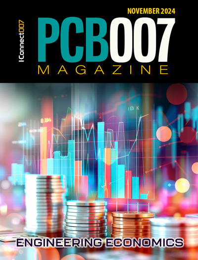
Engineering Economics
The real cost to manufacture a PCB encompasses everything that goes into making the product: the materials and other value-added supplies, machine and personnel costs, and most importantly, your quality. A hard look at real costs seems wholly appropriate.

Alternate Metallization Processes
Traditional electroless copper and electroless copper immersion gold have been primary PCB plating methods for decades. But alternative plating metals and processes have been introduced over the past few years as miniaturization and advanced packaging continue to develop.
- Articles
- Columns
Search Console
- Links
- Media kit
||| MENU - pcb007 Magazine
StratEdge Brings Gold Medal Performance with its Molded Ceramic and Post-fired Ceramic Packages, and High-reliability Assembly Services
August 14, 2024 | StratEdgeEstimated reading time: 1 minute
StratEdge Corporation is redefining the landscape of semiconductor packaging with its cutting-edge molded and post-fired ceramic packages, supported by industry-leading high-reliability assembly services. Engineered to meet the rigorous demands of modern applications, StratEdge's innovative solutions are tailored for markets including telecom, wireless, satellite, defense, and beyond, ensuring unmatched performance in the most challenging environments.
StratEdge's molded ceramic packages offer unparalleled reliability, designed to handle high-frequency chips up to 18 GHz, with over 200 standard outlines available, providing a vast array of packaging options. Complementing these, StratEdge's post-fired ceramic packages excel in thermal management for compound semiconductors like GaN, GaAs, and SiC, operating from DC to 63+ GHz. The packages provide ultra-low loss performance over a wide range of frequencies, depending on the style and mounting configuration. Many open-tooled designs are available with 50 ohm impedance high-frequency transitions, which provide convenience and ease for packaging high-performance semiconductors.
StratEdge's ISO 9001:2015 certified facility features a Class 1000 cleanroom with Class 100 work areas, for performing sensitive microelectronic assembly. It’s equipped with state-of-the-art assembly equipment, including a device bonder with a eutectic gold-tin (AuSn) attachment station that achieves bond line thicknesses of 6µm. This refined eutectic die attach technology maximizes power output for GaN devices, resulting in lower junction temperatures and increased device reliability.
"We manufacture our high-frequency packages with precision, using post-fired ceramics with laser-cut features to control tight tolerances, thermally-enhanced metal bases that dissipate heat, and electrical transition designs that provide exceptionally low electrical losses," explained Casey Krawiec, VP of Global Sales at StratEdge. Krawiec continued, "Working with compound semiconductors, such as GaN, requires a package that can best dissipate the heat from the device while ensuring optimal performance. Although the package plays the most critical part, the way the chip is attached can also make a significant difference in the device's performance."
Suggested Items
The Shaughnessy Report: A Stack of Advanced Packaging Info
12/10/2024 | Andy Shaughnessy -- Column: The Shaughnessy ReportIt’s only fitting that this issue on advanced packaging and stackup features a “stackup” of “packages” on the cover. There’s certainly a lot to “unpack” in this issue. As advanced packaging moves further into the mainstream of PCB design, more PCB designers and design engineers are realizing this isn’t a plug-and-play technology. As we see in this issue, advanced packaging can have an impact on the entire design—the stackup in particular.
ZESTRON South Asia releases whitepaper – Impact of Cleaning Technology on Discrete Packaging - The Difference in Wire Bonding Yield
12/02/2024 | ZESTRONZESTRON, the global leading provider of high precision cleaning products, services, and training solutions in the electronics manufacturing and semiconductor industries, is pleased to release the whitepaper “Impact of Cleaning Technology on Discrete Packaging - The Difference in Wire Bonding Yield”
Würth Elektronik Expands Signal LED Product Range
11/21/2024 | Wurth ElectronicsWürth Elektronik expands its proven LED product series WL-SMCW and WL-SMCC with white LEDs in 0603 and 0402 packages.
Unlock Unmatched Performance for Matched Impedance Devices with StratEdge at IEEE BCICTS 2024
10/22/2024 | StratEdgeStratEdge Corporation, an industry leader in high-frequency and high-power semiconductor packaging, is excited to announce its participation in the IEEE BiCMOS and Compound Semiconductor Integrated Circuits and Technology Symposium (BCICTS).
TopLine to Exhibit 'Drop-in Replacement' for BGA at Electronica
10/16/2024 | TopLineTopLine Corporation will exhibit its latest technology solutions at Electronica in Munich, Germany, November 12 – 15, 2024, in stand B4.428.


