


 Elementary, Mr. Watson: High Power: When Physics Becomes Real
 The Shaughnessy Report: Watt About Power Integrity?
 Global PCB Connections: Understanding Your Fabricator’s Capabilities (or Niche)


Koh Young Showcases Advanced Dimensional Metrology and Inspection Solutions for Semiconductor and Wafer-Level Packaging at SEMICON West
September 3, 2025 | Koh YoungEstimated reading time: 1 minute
Koh Young Technology, the industry leader in True 3D™ measurement-based dimensional metrology and inspection solutions, will present its latest advancements for semiconductor and advanced packaging applications at SEMICON West 2025 in Booth 5949. The show will take place in its new venue at the Phoenix Convention Center from October 7–9, 2025 in Phoenix, Arizona.
With nearly 25,000 systems installed at more than 3,900 manufacturing sites, Koh Young set the standard in automated optical inspection for the electronics manufacturing industry. Building on that foundation, the company expanded into semiconductor manufacturing with higher-resolution optics, advanced measurement algorithms, and solutions engineered for metrology and inspection of wafer-level packages (WLP), system-in-package (SiP), and ultra–high-density interconnect applications.
As an exhibitor, Koh Young will highlight how its AI-powered metrology and inspection solutions help manufacturers meet the exacting demands of advanced packaging and semiconductor processes. From wafer-level to SiP, Koh Young technology delivers accurate, repeatable data to enable smarter process control, drive higher yields, and support zero-defect initiatives.
Proven Platforms for Advanced Packaging Metrology
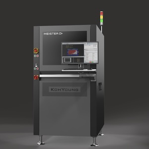
Koh Young’s Meister Series is purpose-built for advanced packaging, including SiP, WLP, and die-stacking metrology. These systems provide ultra-high-resolution 2D/3D measurement to manage features and tolerances in next-generation designs. Complementing the Meister Series, the ZenStar delivers wafer-level dimensional metrology to detect and quantify critical parameters at the earliest stage, ensuring only known-good components advance. Together, these platforms help manufacturers maintain tight process windows, improve yield, and reduce costly rework.
“We are excited about the opportunities SEMICON West brings this year in Phoenix,” said Joel Scutchfield, General Manager of Koh Young America. “The region has long been a center for semiconductor manufacturing, and the recent wave of investment and expansion has only strengthened its position as a hotbed for advanced packaging and innovation. We see tremendous potential for Koh Young to help manufacturers here solve their most pressing challenges. Our mission is to deliver meaningful process insights that improve yield, reduce risk, and give our customers a competitive edge. This show is the perfect forum to collaborate and share how our metrology and inspection solutions can make that vision a reality.”
Share on:


Testimonial
"In a year when every marketing dollar mattered, I chose to keep I-Connect007 in our 2025 plan. Their commitment to high-quality, insightful content aligns with Koh Young’s values and helps readers navigate a changing industry. "
Brent Fischthal - Koh YoungSuggested Items
Pixelworks Announces Definitive Purchase Agreement to Sell its Shanghai Semiconductor Subsidiary to VeriSilicon
10/16/2025 | PRNewswirePixelworks, Inc., a leading provider of innovative video and display processing solutions, today announced that it has signed a definitive agreement to sell its shares in Pixelworks Semiconductor Technology (Shanghai) Co., Ltd., a company organized under the laws of the People's Republic of China and a subsidiary of Pixelworks, to a special purpose entity led by VeriSilicon Microelectronics (Shanghai) Co., Ltd.
DuPont Board of Directors Approves Qnity Distribution
10/16/2025 | QnityDuPont announced that its Board of Directors has approved the previously announced separation of its Electronics business, Qnity Electronics, Inc.
China Expands Rare Earth Export Restrictions, Tightening Grip on Global Supply Chains
10/16/2025 | I-Connect007 Editorial TeamChina sharply expanded its rare earth export restrictions on Oct. 9, adding additional elements and refining technologies to its control list while imposing stricter rules on foreign users in the defense and semiconductor industries.
2H25 Foundry Utilization Exceeds Expectations, Some Players Are Prepared for Price Hikes
10/16/2025 | TrendForceTrendForce’s latest investigations have revealed that wafer foundry utilization during the second half of 2025 has remained more resilient than anticipated. Several factors are contributing to this, including the postponed U.S. semiconductor tariffs, low inventory at IC vendors, the peak smartphone season, and ongoing high demand for AI.
SEMI Foundation, in Partnership with NSF, Opens National RFP for Regional Nodes to Advance Microelectronics Workforce Development
10/15/2025 | SEMIThe SEMI Foundation announced the official opening of the Regional Node Request for Proposals (RFP) for the National Network for Microelectronics Education (NNME), a national initiative funded by the U.S. National Science Foundation (NSF) to accelerate, expand, and improve microelectronics talent development across the United States.