-
- News
- Books
Featured Books
- design007 Magazine
Latest Issues
Current IssueProper Floor Planning
Floor planning decisions can make or break performance, manufacturability, and timelines. This month’s contributors weigh in with their best practices for proper floor planning and specific strategies to get it right.
Showing Some Constraint
A strong design constraint strategy carefully balances a wide range of electrical and manufacturing trade-offs. This month, we explore the key requirements, common challenges, and best practices behind building an effective constraint strategy.
All About That Route
Most designers favor manual routing, but today's interactive autorouters may be changing designers' minds by allowing users more direct control. In this issue, our expert contributors discuss a variety of manual and autorouting strategies.
- Articles
- Columns
- Links
- Media kit
||| MENU - design007 Magazine
Intercept Unveils Enhancements to Pantheon Ink Resistor Technology
September 10, 2015 | Intercept Technology Inc.Estimated reading time: 2 minutes

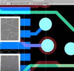
Intercept Technology Inc., a leading EDA software developer for PCB, RF and Hybrid Design solutions today announced powerful and leading-edge enhancements to Pantheon Ink Resistor functionality. In line with Intercept’s mission to provide the highest in advanced design technology, enhancements include the ability to create rectangular as well as complex ink resistor shapes parametrically on the fly during layout, or from information obtained from a schematic. Ink resistor components reside in the design database as parametric types, allowing for flexible modifications as needed at any point during the design process. And, new ink resistor functionality provides users with the ability to manipulate individual ink resistor layers, whether internal or external, creating powerful ink resistor modification capabilities. Defined parametric properties can be saved for use in any design, and users can auto-generate ink resistors based on given inks.
Ink resistor enhancements in Pantheon were built with intuitive graphics and dialogs for the easy setup, generation and modification of ink resistors. Users can create ink resistor shapes either from ink resistor calculation formulas or flexible dialog options as needed. The Ink Resistor Generator Dialog also includes a preview window that updates as ink resistor attributes are modified. And, easy-to-understand graphics help in the specification of such parameters as extensions for overglaze, placement and routing as well as net keepout outlines.
For ink resistor laser trim parameters, Pantheon capabilities provide full functionality with options for passive and functional trim, and additional options are available to specify static and/or dynamic trim clearances for placement and routing. Users can set resistor tolerances and trim percentages for flexibility in ink resistor creation.
“Enhancements to Pantheon’s ink resistor functionality combine the power of Pantheon’s PCB/Hybrid/RF design flow with the intuitive setup and modification of complex ink resistor shapes for the highest advancements in design layout and geometry creation,” said Dale Hanzelka, Director of Sales and Marketing at Intercept. “The resulting software solution provides users with the power to create the highest quality designs in a time of ever-advancing design needs.”
About Intercept
Intercept Technology Inc. is the leading supplier of PCB, RF, hybrid and high speed software solutions for the EDA industry. Intercept's software suite includes PCB schematic and layout design with simulation interfaces, design for manufacture (DFM) rules checking, library management, and 35+ database translators and interfaces that facilitate full environment migration as well as the completion of RF, hybrid, SiP, Analog, Digital, and Mixed-Signal designs. Additionally, Intercept's software solutions are scalable, serving small, medium and large sized companies.
Testimonial
"Our marketing partnership with I-Connect007 is already delivering. Just a day after our press release went live, we received a direct inquiry about our updated products!"
Rachael Temple - AlltematedSuggested Items
Global PCB Connections: Understanding the General Fabrication Process—A Designer’s Hidden Advantage
08/14/2025 | Markus Voeltz -- Column: Global PCB ConnectionsDesigners don’t need to become fabricators, but understanding the basics of PCB fabrication can save you time, money, and frustration. The more you understand what’s happening on the shop floor, the better you’ll be able to prevent downstream issues. As you move into more advanced designs like HDI, flex circuits, stacked vias, and embedded components, this foundational knowledge becomes even more critical. Remember: the fabricator is your partner.
The Art and Science of PCB Floor Planning: A Comprehensive Guide
08/14/2025 | Cory Grunwald and Jeff Reinhold, Monsoon SolutionsPCB design is an intricate and crucial part of developing electronic products. One of the foundational stages of PCB design is floor planning, a phase where the placement of components and the flow of signals are meticulously mapped out. A good floor plan ensures that the PCB performs well, is easy to manufacture, and meets all mechanical and electrical requirements. We’ll explore the essential aspects of floor planning, from its objectives and process to the challenges that designers face.
EnSilica Establishes New EU Mixed-Signal Design Centre in Budapest, Hungary
08/12/2025 | EnSilicaThe facility strengthens EnSilica’s presence in the European Union and taps into Budapest’s deep technology ecosystem, which hosts numerous leading automotive and industrial multinationals. This expansion will increase the Group’s global headcount to around 210 employees.
Happy’s Tech Talk #41: Sustainability and Circularity for Electronics Manufacturing
08/13/2025 | Happy Holden -- Column: Happy’s Tech TalkI attended INEMI’s June 12 online seminar, “Sustainable Electronics Tech Topic Series: PCBs and Sustainability.” Dr. Maarten Cauwe of imec spoke on “Life Cycle Inventory (LCI) Models for Assessing and Improving the Environmental Impact of PCB Assemblies,” and Jack Herring of Jiva Materials Ltd. spoke on “Transforming Electronics with Recyclable PCB Technology.” This column will review information and provide analysis from both presentations.
Elementary, Mr. Watson: Why Your PCB Looks Like a Studio Apartment
08/13/2025 | John Watson -- Column: Elementary, Mr. WatsonIn November 2022, I wrote a column called "Is Your Bathroom in the Kitchen?" This piece related a bizarre real estate listing that emerged out of St. Louis that had architects scratching their heads and interior designers cringing. Nestled in the historic Central West End sat a 200-square-foot apartment that completely defied logic. It wasn't the size that raised eyebrows, it was the layout. Here's the kicker: While that's rare in real estate, it's shockingly common in PCB design.