


 Dan’s Biz Bookshelf: Four Important Books You Need to Read (Not Just Say You Have)
 The Marketing Minute: Cracking the Code of Technical Marketing


Nature-Inspired Nanotubes That Assemble Themselves, With Precision
March 29, 2016 | Lawrence Berkeley National LaboratoryEstimated reading time: 4 minutes
When it comes to the various nanowidgets scientists are developing, nanotubes are especially intriguing. That’s because hollow tubes that have diameters of only a few billionths of a meter have the potential to be incredibly useful, from delivering cancer-fighting drugs inside cells to desalinating seawater.
But building nanostructures is difficult. And creating a large quantity of nanostructures with the same trait, such as millions of nanotubes with identical diameters, is even more difficult. This kind of precision manufacturing is needed to create the nanotechnologies of tomorrow.
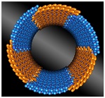
Help could be on the way. As reported online this week in the journal Proceedings of the National Academy of Sciences, researchers at the U.S. Department of Energy’s Lawrence Berkeley National Laboratory (Berkeley Lab) have discovered a family of nature-inspired polymers that, when placed in water, spontaneously assemble into hollow crystalline nanotubes. What’s more, the nanotubes can be tuned to all have the same diameter of between five and ten nanometers, depending on the length of the polymer chain.
The polymers have two chemically distinct blocks that are the same size and shape. The scientists learned these blocks act like molecular tiles that form rings, which stack together to form nanotubes up to 100 nanometers long, all with the same diameter.
“This points to a new way we can use synthetic polymers to create complex nanostructures in a very precise way,” says Ron Zuckermann, who directs the Biological Nanostructures Facility in Berkeley Lab’s Molecular Foundry, where much of this research was conducted.
Several other Berkeley Lab scientists contributed to this research, including Nitash Balsara of the Materials Sciences Division and Ken Downing of the Molecular Biophysics and Integrated Bioimaging Division.
“Creating uniform structures in high yield is a goal in nanotechnology,” adds Zuckermann. “For example, if you can control the diameter of nanotubes, and the chemical groups exposed in their interior, then you can control what goes through—which could lead to new filtration and desalination technologies, to name a few examples.”
The research is the latest in the effort to build nanostructures that approach the complexity and function of nature’s proteins, but are made of durable materials. In this work, the Berkeley Lab scientists studied a polymer that is a member of the peptoid family. Peptoids are rugged synthetic polymers that mimic peptides, which nature uses to form proteins. They can be tuned at the atomic scale to carry out specific functions.
For the past several years, the scientists have studied a particular type of peptoid, called a diblock copolypeptoid, because it binds with lithium ions and could be used as a battery electrolyte. Along the way, they serendipitously found the compounds form nanotubes in water. How exactly these nanotubes form has yet to be determined, but this latest research sheds light on their structure, and hints at a new design principle that could be used to build nanotubes and other complex nanostructures.
Page 1 of 2
Share on:


Testimonial
"We’re proud to call I-Connect007 a trusted partner. Their innovative approach and industry insight made our podcast collaboration a success by connecting us with the right audience and delivering real results."
Julia McCaffrey - NCAB GroupSuggested Items
MEMS & Imaging Sensors Summit to Spotlight Sensing Revolution for Europe’s Leadership
09/11/2025 | SEMIIndustry experts will gather November 19-20 at the SEMI MEMS & Imaging Sensors Summit 2025 to explore the latest breakthroughs in AI-driven MEMS and imaging optimization, AR/VR technologies, and advanced sensor solutions for critical defence applications.
Direct Imaging System Market Size to Hit $4.30B by 2032, Driven by Increasing Demand for High-Precision PCB Manufacturing
09/11/2025 | Globe NewswireAccording to the SNS Insider, “The Direct Imaging System Market size was valued at $2.21 Billion in 2024 and is projected to reach $4.30 Billion by 2032, growing at a CAGR of 8.68% during 2025-2032.”
I-Connect007’s Editor’s Choice: Five Must-Reads for the Week
07/04/2025 | Marcy LaRont, I-Connect007For our industry, we have seen several bullish market announcements over the past few weeks, including one this week by IDC on the massive growth in the global server market. We’re also closely watching global trade and nearshoring. One good example of successful nearshoring is Rehm Thermal Systems, which celebrates its 10th anniversary in Mexico and the official opening of its new building in Guadalajara.
Driving Innovation: Direct Imaging vs. Conventional Exposure
07/01/2025 | Simon Khesin -- Column: Driving InnovationMy first camera used Kodak film. I even experimented with developing photos in the bathroom, though I usually dropped the film off at a Kodak center and received the prints two weeks later, only to discover that some images were out of focus or poorly framed. Today, every smartphone contains a high-quality camera capable of producing stunning images instantly.
United Electronics Corporation Advances Manufacturing Capabilities with Schmoll MDI-ST Imaging Equipment
06/24/2025 | United Electronics CorporationUnited Electronics Corporation has successfully installed the advanced Schmoll MDI-ST (XL) imaging equipment at their advanced printed circuit board facility. This significant technology investment represents a continued commitment to delivering superior products and maintaining their position as an industry leader in precision PCB manufacturing.