


 Learning with Leo: Drones—Meeting Demand Without Compromise
 Nolan’s Notes: Our Spotlight on North America
 Global Sourcing Spotlight: Building a Supply Chain That Bends, Not Breaks


Scientists Study the Insulator-Superconductor Transition of Copper-Oxide Compound in Fine Detail
April 11, 2016 | BNLEstimated reading time: 4 minutes
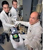
Using a highly controlled deposition technique, scientists from the U.S. Department of Energy's (DOE) Brookhaven National Laboratory have synthesized ultrathin films containing multiple samples of a copper-oxide compound to study the compound's electronic behavior at near absolute zero, or minus 459 degrees Fahrenheit. This technique, as described in a paper published in this week's Online Early Edition of the Proceedings of the National Academy of Sciences, is helping scientists understand how electrons behave as this material transitions from being an insulator to a superconductor capable of carrying electric current with no resistance.
"We are trying to understand the mechanism of the insulator-superconductor transition in a family of compounds called the cuprates. These compounds become superconducting at relatively high temperatures—minus 200 degrees Fahrenheit—in comparison to most superconducting materials, which require temperatures within a few degrees of absolute zero," said Jie Wu, lead author on the paper and a physicist in Brookhaven Lab's Condensed Matter Physics and Materials Science Department. "Characterizing this mechanism may provide insight into how we can make the superconducting temperature even higher, possibly even reaching room temperature."
This capability would enable electricity to be transferred much more efficiently. "Imagine a power line that carries electricity without any energy loss. We could wire the whole planet, resulting in trillions of dollars in savings and reduced environmental impact," said Wu.
Insulator-superconductor transition
In their native state, cuprates are insulators; they do not readily conduct electricity. But cuprates can become superconducting when chemically "doped" with strontium atoms, which produce free-moving electrons that pair up in the crystalline copper-oxide layers where superconductivity is known to occur.
At a certain reduced doping level, however, superconductivity weakens and eventually disappears. As the cuprates' superconducting temperature is lowered to near absolute zero, resistance increases somewhat (a characteristic of insulators) yet conductivity remains quite high (a characteristic of metals). The nature of this strange "insulating" state has been a puzzle to scientists for years.
Solving the puzzle requires a method of fine-tuning the doping level to incrementally approach the quantum critical point—the "tipping" point at which a material is on the cusp of transitioning from one state of electronic order to another, similar to the phase change that happens when ice melts into liquid water. It also requires a highly sensitive way to measure the electronic changes corresponding with the different doping levels.
One film, many samples
To study the insulator-superconductor transition in fine detail, the scientists synthesized films of a compound containing lanthanum, strontium, copper, and oxygen. They used a combinatorial molecular beam epitaxy system at Brookhaven that places materials onto a substrate, atom by atom, in a layered manner and at tightly controlled deposition rates.
Through photolithography, a technique of transferring a geometric pattern onto a substrate, the scientists patterned single-crystal films into a linear "combinatorial" library containing 30 samples, each with a slightly different chemical doping level near the quantum critical point. To provide the electrical contact needed to measure the resistivity of the samples, they evaporated gold pads onto the films' surface.
"We programmed the system to vary the doping level continuously and very precisely at a set minute increment," said Ivan Bozovic, co-author on the paper and a senior physicist in Brookhaven's Condensed Matter Physics and Materials Science Department.
The scientists then measured the electrical resistivity of the samples with varying temperatures, magnetic fields, and doping levels near the quantum critical point. Two types of measurements were taken: one parallel to the electrical current (longitudinal resistivity) and one perpendicular (Hall resistivity).
"The Hall resistivity is much more sensitive because it measures the voltage at a particular cross section of the sample. Longitudinal resistivity averages the whole section," said Wu. "Our Brookhaven team is the first to use this more localized approach that can give us a direct measurement of the density of mobile electrons."
Page 1 of 2
Share on:


Testimonial
"We’re proud to call I-Connect007 a trusted partner. Their innovative approach and industry insight made our podcast collaboration a success by connecting us with the right audience and delivering real results."
Julia McCaffrey - NCAB GroupSuggested Items
Driving Innovation: Selecting the Right Laser Source
04/28/2026 | Simon Khesin -- Column: Driving InnovationWhen I first joined Schmoll Maschinen, I brought experience from almost every PCB process, except for laser. As I immersed myself in laser processing, I realized why it can seem so daunting to a newcomer. The complexity arises from three intersecting factors: A vast variety of laser sources: CO2, UV-nano, green-pico, UV-pico, IR-pico, and others; a diverse range of applications: Drilling, cutting, ablation, and more; and an extensive list of materials: These have vastly different absorption rates. Choosing the right machine or laser source is rarely trivial. Even for experienced engineers, answering "Which source is best?" requires examining the business's specific goals.
Institute of Circuit Technology Spring Seminar 2026: A Bright Future in Europe
04/23/2026 | Pete Starkey, I-Connect007Through the leafy lanes and spring flowers of Warwickshire and back to Meridan, the traditional centre of England, and now officially part of the Metropolitan Borough of Solihull in the county of the West Midlands, I attended the Annual General Meeting and Spring Seminar of the Institute of Circuit Technology (ICT) on April 14. Out of the AGM came notable changes in leadership at the top of the Institute: the retirement of Mat Beadel as chair and Emma Hudson as technical director. Effective May 1, Steve Driver is the new chair, and Alun Morgan is the new technical director.
ACCM Unveils Negative and Near-zero CTE Materials for Large-Format AI Chips
04/21/2026 | Advanced Chip and Circuit MaterialsAdvanced Chip and Circuit Materials, Inc. (ACCM) has launched two new materials: Celeritas HM50, with a negative coefficient of thermal expansion (CTE) of -8 ppm/°C to offset the positive CTE and expansion of copper with temperature on circuit boards, and Celeritas HM001, with near-zero CTE and the low-loss performance needed for high-speed signal layers to 224 Gb/s and faster in artificial intelligence (AI) circuits.
Fresh PCB Concepts: Designing PCBs for Harsh Environments—Reliability Is Engineered Upstream
04/23/2026 | Team NCAB -- Column: Fresh PCB ConceptsWhen engineers hear the phrase “harsh environment,” they usually think of the extreme temperature swings, vibration and shock, pressure changes, or radiation in aerospace. However, aerospace is not the only harsh environment where electronic assemblies must survive. Automotive power electronics, downhole oil and gas tools, marine controls, rail systems, defense platforms, and industrial automation equipment all expose PCBs to environments that are equally unforgiving. The stress mechanisms may differ, but the physics does not.
Advanced Packaging for AI: Reliability Starts at the Cu/Cu/Cu Microvia Junction
04/20/2026 | Kuldip Johal, MKS' AtotechThe rapid growth of AI computing, from training clusters to inference at scale, is reshaping demand across the entire electronics supply chain. Advances in technology requirements, such as higher bandwidth, lower latency, and greater compute density, are driving the development of advanced packaging technologies and transforming the PCB industry across design, manufacturing, testing, and even architecture.