


 Target Condition: The Modern Masters of Signal Integrity and AI-driven Design
 Fresh PCB Concepts: Repair and Risk in Electrical Test Failures in PCB Manufacturing
 Elementary, Mr. Watson: The Design Matrix—Revealing the Hidden Truths of Reality


In recent years, the miniaturization and modularization of electronic products have led to the increased density of electronic components and the decrease of areas for effective heat dissipation. As a result, the thermal design of high-powered electronic components has become a major focus for electronics engineers. An effective solution for FPGA heat dissipation is critical. Thermal design of the PCB aims to decrease the temperature of both components and the board through suitable measures, so that the system is capable of working at a suitable temperature.
There are numerous available methods for dealing with heat dissipation, but their cost and practicability have yet to be fully considered. Based on an analysis of practical heat dissipation issues, this article provides thermal design tips for PCBs that feature FPGAs.
FPGA and Heat Dissipation Issues
A type of FPGA PCB is designed for teaching and research applications, consisting of a host chip FPGA, +3.3V and +1.2V power circuit, 50MHz clock circuit, reset circuit, JTAG and AS download interface circuit, SRAM memory and interface introduced by I/O. The EP3C5E144C7 is applied as an FPGA host master chip with QFP package in this research. The system structure of a PCB with FPGA as a core is shown in Figure 1.
Figure 1: Structure of an FPGA control system.
Heat sources on a PCB with FPGA as a core derive primarily from these drivers:
● The PCB requires a power supply of +5V, +3.3V and +1.2V, and the power module produces high heat when it is functioning. If effective measures aren’t taken in time, power module will become so hot that it fails to work normally.
● The FPGA features a clock frequency of 50MHz and the PCB features a large routing density. Since the improvement of system integrity leads to relatively high system energy consumption, necessary heat dissipation measures are required to be made.
● The PCB produces its own heat. Copper conductor is a basic material for PCB prototyping, and heat is generated as a result of the current exchange and energy consumption of copper conductor corrosion lines, which act as built-in resistors.
Thermal Design for PCBs with an FPGA Core
Thermal Power Design
External DC power of +5V is accessed to the PCB, requiring a current of more than 1A. An LDO LT1117 chip is picked up by a power module, transforming +5V DC power into +3.3V VCCIO port voltage required by EP3C5E144C7 and +1.2V VCCINT Vcore. The LT1117 is housed in an SOT-23 SMT package.
Based on the analysis mentioned earlier, two LT1117 chips are required in order to meet the supply requirement of +3.3V and +1.2V necessary for the FPGA. Thermal design measures for power module in the process of PCB design include:
A. Since heat is generated by the power module after much usage, a certain distance should be maintained between adjacent power modules during layout. Since too small a distance between adjacent power modules can cause heat dissipation, the distance between the LDO chip and LT1117 should be set to be 20mm or more.
B. Copper coating can be implemented independently at the position where the LDO chip and LT1117 are placed, which is beneficial for heat dissipation. This is shown in Figure 2.
Figure 2: Copper coating at bottom of power module for greater heat dissipation.
c. When necessary, cooling fins can be added to the LDO chip in order to ensure the fast heat dissipation of power module and provide normal power for the FPGA chip.
Through-Hole Via Design for Heat Dissipation
Some heat conductive metal through-hole vias should be placed at the bottom of and around components with large heat generation. These should be small vias with a diameter of 0.4mm to 1mm that go through the PCB. The vias’ diameter shouldn’t be too large, and the distance between vias should be in the range of1mm to 1.2mm. Through-hole vias conduct the heat from the front of the PCB to the heat dissipation layers along the back of PCB. The components will be cooled quickly at the thermal side of the PCB, effectively increasing the dissipation area and improving the power density of the circuits. Proper thermal design for metal through-hole vias is shown in Figure 3.
Figure 3: Heat dissipation of through-hole vias.
FPGA Thermal Design
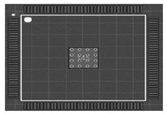
FPGA heat derives mainly from dynamic energy consumption, from sources such as Vcore, I/O voltage, memory, internal logic, and system energy consumption produced when the FPGA controls other function modules, such as video and audio. With the generation of heat, it’s necessary to implement thermal design on the FPGA chip. In the process of QFP package design for FPGAs, a 4.5mm×4.5mm piece of copper foil is added to the center of the FPGA chip and a certain number of heat dissipation pads are designed with cooling fins that can be added according to practical requirements. The thermal design for an FPGA is illustrated in Figure 4.
Figure 4: Thermal design for FPGAs.
Thermal design for copper coating
Copper coating on a PCB not only increases the anti-interference of the circuit, but also effectively improves the heat dissipation of the PCB. Generally, there are two types of copper coating methods available in the Altium Designer Summer 09 release: a large area copper coating and grid copper coating. The essential defect of large-scale strip copper coating is that relatively high heat is generated when PCB is functioning for a long time so that strip copper coating will possibly expand and fall off. Therefore, it’s better to apply grid copper coating for heat dissipation. Grounding network communication between grid and circuit should be set to increase the shielding effect and heat dissipation of the system. Thermal design for copper coating of FPGA is displayed in Figure 5.
Figure 5: Thermal design for copper coating.
Conclusion
Thermal design of the PCB is the key link to ensuring the stability and reliability of the PCB, and the selection of heat dissipation methods is the first element for consideration. The best heat dissipation methods for FPGAs feature properties of high practicability, low cost and easy implementation.
Dora Yang is an electronics engineer with PCBCart, a China-based custom PCB fabrication, assembly and parts sourcing services provider.


