


 It’s Only Common Sense: Selling Without Selling
 Dan’s Biz Bookshelf: ‘The Art of Going SLOW’
 Happy’s Tech Talk #39: PCBs Replace Motor Windings


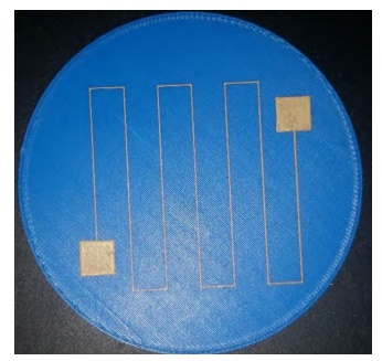
3D Printed Electronics for Printed Circuit Structures
October 4, 2017 | Samuel LeBlanc, Paul Deffenbaugh, Jacob Denkins, and Kenneth Church nSCRYPT INC.Estimated reading time: 1 minute
Abstract
Printed electronics is a familiar term that is taking on more meaning as the technology matures. Flexible electronics is sometimes referred to as a subset of this and the printing approach is one of the enabling factors for roll-to-roll processes. Printed electronics is improving in performance and has many applications that compete directly with printed circuit boards. The advantage of roll-to-roll is the speed of manufacturing, the large areas possible, and a reduction in costs.
As this technology continues to mature, it is also merging with the high-profile 3D printing. 3D printing is becoming more than just a rapid prototyping tool and more than just printing small plastic toys. Companies are embracing 3D printing as a manufacturing approach to fabricate complex parts that cannot be done using traditional manufacturing techniques. The combination of 3D printing and printed electronics has the potential to make novel products and, more specifically, to make objects electrically functional. Electrically functional objects have the advantage of competing with printed circuit boards.
Printed circuit structures will be a new approach to electronic packaging. It is the desire of many companies to reduce assembly processes, decrease the size of the electronics, and do this at a reduced cost. This is challenging, but the potential of printing the structure and the electronics as a single monolithic unit has many advantages. This will reduce the human touch in assembly, as the electronics and the object are printed. This will increase the ruggedness of the product, as it is a monolithic device.
This will eliminate wires, solder, and connectors, making the device smaller. This has the potential to be the future of printed circuit boards and microelectronic packaging. This article will show working demonstrations of printed circuit structures, the obstacles, and the potential future of 3D printed electronics.
To read the full version of this article which appeared in the September 2017 issue of The PCB Magazine, click here.
Share on:


Suggested Items
Preventing Surface Prep Defects and Ensuring Reliability
06/10/2025 | Marcy LaRont, PCB007 MagazineIn printed circuit board (PCB) fabrication, surface preparation is a critical process that ensures strong adhesion, reliable plating, and long-term product performance. Without proper surface treatment, manufacturers may encounter defects such as delamination, poor solder mask adhesion, and plating failures. This article examines key surface preparation techniques, common defects resulting from improper processes, and real-world case studies that illustrate best practices.
Breaking Silos with Intelligence: Connectivity of Component-level Data Across the SMT Line
06/09/2025 | Dr. Eyal Weiss, CybordAs the complexity and demands of electronics manufacturing continue to rise, the smart factory is no longer a distant vision; it has become a necessity. While machine connectivity and line-level data integration have gained traction in recent years, one of the most overlooked opportunities lies in the component itself. Specifically, in the data captured just milliseconds before a component is placed onto the PCB, which often goes unexamined and is permanently lost once reflow begins.
BEST Inc. Introduces StikNPeel Rework Stencil for Fast, Simple and Reliable Solder Paste Printing
06/02/2025 | BEST Inc.BEST Inc., a leader in electronic component rework services, training, and products is pleased to introduce StikNPeel™ rework stencils. This innovative product is designed for printing solder paste for placement of gull wing devices such as quad flat packs (QFPs) or bottom terminated components.
See TopLine’s Next Gen Braided Solder Column Technology at SPACE TECH EXPO 2025
05/28/2025 | TopLineAerospace and Defense applications in demanding environments have a solution now in TopLine’s Braided Solder Columns, which can withstand the rigors of deep space cold and cryogenic environments.
INEMI Interim Report: Interconnection Modeling and Simulation Results for Low-Temp Materials in First-Level Interconnect
05/30/2025 | iNEMIOne of the greatest challenges of integrating different types of silicon, memory, and other extended processing units (XPUs) in a single package is in attaching these various types of chips in a reliable way.