


 Elementary, Mr. Watson: Heat—The Hidden Villain of Power Electronics
 Beyond Design: The Fundamental Structure of Spectral Integrity
 The Shaughnessy Report: Watt About Power Integrity?


Focusing on Surface Sensitivity for Reliability
August 20, 2019 | Andy Shaughnessy, I-Connect007Estimated reading time: 3 minutes
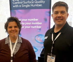
During the IPC High-Reliability Forum and Microvia Summit, I spoke with Customer Applications Scientist Elizabeth Kidd and Sales Engineer Alex Bien, both of BTG Labs, about their presentation on the challenges of working with highly sensitive surfaces, such as the risk of contamination. We also discussed the various surface characterization techniques that BTG Labs uses to identify such contaminants, and some PCB design strategies for creating a better surface—and a more reliable board.
Andy Shaughnessy: Elizabeth, it’s nice to meet you. I know you’re giving a presentation in a few days, but tell us about the company, and then we’ll talk about your presentation.
Elizabeth Kidd: Sure. BTG labs is a materials science company specializing in surface science and adhesion technologies. We have our roots in being a research and development lab and scoping root cause analyses for people who are scratching their heads at these industrial adhesion problems. From there, we develop the technology to make manufacturing floor inspections of materials as they go through their critical surface process points.
Alex Bien: We help folks to hone in on one area—the surface—that they’ve never had eyes on nor had a way to quickly evaluate surface chemistry in a fast, point-and-shoot manner. Our opening speaker today is addressing this lack of insight into the three nanometers that we need to control to create reliable adhesion. Thus, our focus is putting that technology to the floor in the hands of people who are making dollars-and-cents decisions every day.
Kidd: And taking the high sensitivity of R&D techniques—such as XPS, X-ray photoelectron spectroscopy, and FTIR, which is Fourier transform infrared spectroscopy—that have their eyes on the top molecular layer of a surface, and being able to scale that to a method or technique that can be taken onto the manufacturing floor.
Shaughnessy: Can you also tell us about your presentation?
Kidd: The presentation addressed what we just mentioned—controlling your surface process to better your wire bonding, die pad bonding, laminate coating adhesion, and all of those things. We even have some applications for the coupling agents that we were speaking of known as a conversion coating, and other industries use those organosilanes to increase adhesion between organic material and inorganic material.
Shaughnessy: Are you talking about copper, FR-4, and any sort of surface?
Kidd: Yes. We’ll have some applications in metallics, polymers, and in composites as well.
Bien: That’s a good point, though. It’s particularly difficult to control surface chemistry and match surface chemistry between dissimilar materials. It’s very easy to bond metal to metal, and it’s pretty easy to bond composite to composite, but metal to polymer, glass to polymer, and those material interfaces are more challenging to create to promote adhesion.
Shaughnessy: What are the biggest takeaways from your talk?
Kidd: Namely, the sensitivity of this surface. As Alex mentioned, we have a monomolecular layer that we’re trying to control, and that layer is highly sensitive to contamination events. Contact contaminants from the manufacturing process—things like upstream process aids from stamping or anything left over from any wash process from a chemical etch bath—have a huge impact. Or perhaps you’ve had a change in your supply chain where supplier X used chemical X, and now supplier Y is using chemical Y, and all of a sudden, you have more random failures or successes, and you don’t know why.
It’s drawing attention to those small changes in a process that can affect that monolayer that we’re trying to adhere to. We’ll mainly be talking about contamination, how to look for it, how to characterize that, using various surface characterization techniques—such as FTIR, XPS, and contact angle measurements—and surface activation and detection of coatings. The main takeaway is to increase the awareness of the sensitivity and how you can change—negatively or positively—that surface, even unknowingly.
Shaughnessy: With one small thing having a large influence on the process.
Bien: A small change in the process creates a snowball effect downstream.
Kidd: Exactly. Think about a fingerprint. If you put a fingerprint on the surface, that’s 1,000–10,000 molecules thick. If you try to stick something to it now, you’re not sticking to the surface; you’re sticking to the chemicals and the oil from that person’s fingers. That kind of sensitivity is important.
To read the full article, which appeared in the July 2019 issue of PCB007 Magazine, click here.
Share on:


Testimonial
"The I-Connect007 team is outstanding—kind, responsive, and a true marketing partner. Their design team created fresh, eye-catching ads, and their editorial support polished our content to let our brand shine. Thank you all! "
Sweeney Ng - CEE PCBSuggested Items
Episode 6 of Ultra HDI Podcast Series Explores Copper-filled Microvias in Advanced PCB Design and Fabrication
10/15/2025 | I-Connect007I-Connect007 has released Episode 6 of its acclaimed On the Line with... American Standard Circuits: Ultra High Density Interconnect (UHDI) podcast series. In this episode, “Copper Filling of Vias,” host Nolan Johnson once again welcomes John Johnson, Director of Quality and Advanced Technology at American Standard Circuits, for a deep dive into the pros and cons of copper plating microvias—from both the fabricator’s and designer’s perspectives.
Nolan’s Notes: Tariffs, Technologies, and Optimization
10/01/2025 | Nolan Johnson -- Column: Nolan's NotesLast month, SMT007 Magazine spotlighted India, and boy, did we pick a good time to do so. Tariff and trade news involving India was breaking like a storm surge. The U.S. tariffs shifted India from one of the most favorable trade agreements to the least favorable. Electronics continue to be exempt for the time being, but lest you think that we’re free and clear because we manufacture electronics, steel and aluminum are specifically called out at the 50% tariff levels.
MacDermid Alpha & Graphic PLC Lead UK’s First Horizontal Electroless Copper Installation
09/30/2025 | MacDermid Alpha & Graphic PLCMacDermid Alpha Electronics Solutions, a leading supplier of integrated materials and chemistries to the electronics industry, is proud to support Graphic PLC, a Somacis company, with the installation of the first horizontal electroless copper metallization process in the UK.
Electrodeposited Copper Foils Market to Grow by $11.7 Billion Over 2025-2032
09/18/2025 | Globe NewswireThe global electrodeposited copper foils market is poised for dynamic growth, driven by the rising adoption in advanced electronics and renewable energy storage solutions.
MacDermid Alpha Showcases Advanced Interconnect Solutions at PCIM Asia 2025
09/18/2025 | MacDermid Alpha Electronics SolutionsMacDermid Alpha Electronic Solutions, a global leader in materials for power electronics and semiconductor assembly, will showcase its latest interconnect innovations in electronic interconnect materials at PCIM Asia 2025, held from September 24 to 26 at the Shanghai New International Expo Centre, Booth N5-E30