-

- News
- Books
Featured Books
- design007 Magazine
Latest Issues
Current Issue
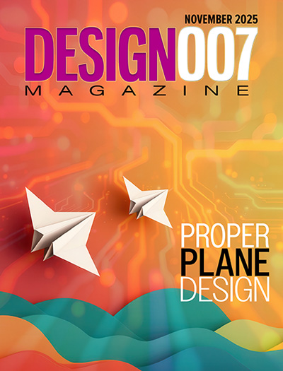
Designing Proper Planes
Without planes, designers would have to create thousands of traces to accomplish the same objectives. Power planes provide low impedance and stable power, and ground planes stabilize reference voltage, improve thermal performance, and help preclude EMI issues.

Power Integrity
Current power demands are increasing, especially with AI, 5G, and EV chips. This month, our experts share “watt’s up” with power integrity, from planning and layout through measurement and manufacturing.

Signal Integrity
If you don’t have signal integrity problems now, you will eventually. This month, our expert contributors share a variety of SI techniques that can help designers avoid ground bounce, crosstalk, parasitic issues, and much more.
- Articles
- Columns
- Links
- Media kit
||| MENU - design007 Magazine
Component Selection for Easier Design and Manufacture of Electronics
December 17, 2014 | Joe Fjelstad, Verdant ElectronicsEstimated reading time: 1 minute
“Simplify, simplify, simplify.”
—Henry David Thoreau
Thoreau penned his simple lifestyle mantra more than 150 years ago and it still as valid today as it was when he first captured and recorded his thoughts on paper. He was not the first to extoll the importance of simplicity, but he said it in a memorable way.
Achieving simplicity has been deemed a worthy objective by many philosophers over centuries, and people often profess to seek simplicity in their lives. In the world of high tech, simplicity is arguably one of the foundational objectives of most of the technologies that surround us today. Certainly this is true in terms of how product designers are trying to create interfaces that allow even the most nontechnical users to get what they need from electronic products with a minimum of hassle.
However, that interface simplicity is undergirded by a massively complex electromechanical substructure of circuits, sensors and components. Pop open any high-end electronic device and you will be met by an impressive mass of densely packed components and circuits. Presently, those components are available in a wide array of formats, with a number of different lead shapes and forms along with the device’s mechanical outline. Presently, there are J-leads, I-leads, gull-wing leads, posts, balls and no leads at all. Mechanical outlines are generally square and rectangular, but the bodies can have a wide range of dimensions in X, Y and Z. While area array technology has helped to make things smaller, it has also upped the complexity factor from a design perspective by mixing grids and land shapes and sizes.
Why so many options? It is because there is not, nor has there ever been, a truly coherent approach to the process of selecting package structures for ICs or any other components for that matter. Yes, a roadmap for electronic component lead pitch was introduced with the advent of SMT, and that roadmap said that every next-generation lead pitch should be 80% of the size of the previous generation lead pitch.
Read the full article here.
Editor's Note: This article originally appeared in the November 2014 issue of The PCB Design Magazine.
Testimonial
"Your magazines are a great platform for people to exchange knowledge. Thank you for the work that you do."
Simon Khesin - Schmoll MaschinenSuggested Items
PCB Design Software Market to Hit $12.11 Billion by 2033, Growing at a CAGR of 13.77%
11/14/2025 | Globe NewswireThe PCB Design Software Market Size was valued at USD 4.32 Billion in 2025E and is expected to reach USD 12.11 Billion by 2033 and grow at a CAGR of 13.77% over the forecast period 2026-2033.
Zuken Opens Call for Papers for ZIW Americas 2026
11/13/2025 | ZukenZuken USA, Inc. opens the Zuken Innovation World (ZIW) Americas 2026 Call for Papers to help engineers, managers, and leaders showcase proven results and advance industry best practices. ZIW is Zuken USA’s semi-annual Digital Engineering conference on electrical and electronic design for engineers, managers, and industry leaders. It focuses on current practices and emerging trends with practical takeaways.
Innatera Signs Joya as ODM Customer, Bringing Neuromorphic Edge AI into Everyday Connected Products
11/13/2025 | PRNewswireInnatera, the leader in brain-like neuromorphic computing for ultra-low-power intelligence at the sensor edge, today announced that Xiamen Joyatech Co., Ltd. has become its first Original Design Manufacturer (ODM) customer.
Advanced Electronics Packaging Digest: Third Issue Arrives November 17
11/12/2025 | I-Connect007The third issue of Advanced Electronics Packaging Digest launches Monday, November 17. This issue continues AEPD’s mission to deliver forward-looking analysis and insider perspectives on the technologies reshaping advanced electronics packaging. Among the highlights is a review of IMPACT 2025, where discussions on component-to-system-level integration took center stage as experts explored the challenges and breakthroughs driving advanced packaging technologies.
Electronic Design Automation (EDA) Market Size to Reach $811.1 Million by 2030
11/12/2025 | PRNewswireThe Global Electronic Design Automation (EDA) Market was estimated to be worth USD 541 Million in 2023 and is forecast to a readjusted size of USD 811.1 Million by 2030 with a CAGR of 6.4% during the forecast period 2024-2030.


