-

- News
- Books
Featured Books
- smt007 Magazine
Latest Issues
Current Issue
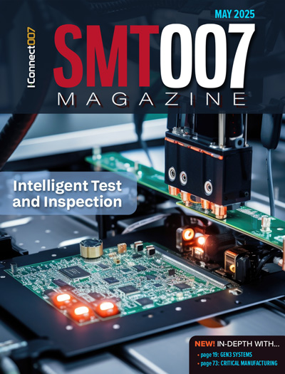
Intelligent Test and Inspection
Are you ready to explore the cutting-edge advancements shaping the electronics manufacturing industry? The May 2025 issue of SMT007 Magazine is packed with insights, innovations, and expert perspectives that you won’t want to miss.

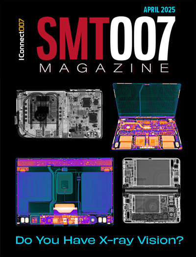
Do You Have X-ray Vision?
Has X-ray’s time finally come in electronics manufacturing? Join us in this issue of SMT007 Magazine, where we answer this question and others to bring more efficiency to your bottom line.

IPC APEX EXPO 2025: A Preview
It’s that time again. If you’re going to Anaheim for IPC APEX EXPO 2025, we’ll see you there. In the meantime, consider this issue of SMT007 Magazine to be your golden ticket to planning the show.
- Articles
- Columns
Search Console
- Links
- Media kit
||| MENU - smt007 Magazine
Reflow Profiling on the Electrical Reliability of No-Clean Solder Paste Flux Residues
May 5, 2015 | By Eric Bastow, Indium Corp.Estimated reading time: 2 minutes
An estimated 80% of all SMT assembly in the world is performed with a no-clean soldering process, largely due to the predominance of consumer electronics. The continuing trend of increasing miniaturization that dominates modern electronics devices requires no-clean flux residues to be as benign and electrically resistive as possible. Solder pastes with an IPC J-STD-004[1] classification of ROL0 or ROL1 rely heavily on two basic mechanisms to render the flux residue as "no-clean": (1) the encapsulating properties that the rosin provides and (2) the heat activation/decomposition of the chemicals in the flux, commonly known as “activators.” The latter is generally known in the industry, but is rarely taken into consideration for reflow profiling in SMT assembly.
Optimization of a reflow profile often focuses on mitigating defects such as voiding, tombstoning, graping, slumping/bridging, etc. However, little thought is given to the reflow profile’s effect on the electrical reliability of the no-clean flux residue. Because of the wide variation in size and thermal density of SMT components and PCBs, achieving a reflow profile that equally heats the entire assembly can be challenging and often impossible. The temperature under a large component, such as a BGA, is often markedly cooler than a smaller component, such as a passive resistor or capacitor. This paper will discuss an experiment that studied the effect of reflow profiling on the electrical reliability of no-clean flux residues that can be measured using IPC J-STD-004[1] surface insulation resistance (SIR) testing. Both a halogen-free (ROL0) and a halogen-containing (ROL1) Pb-free no-clean solder paste, exposed to various reflow profiles, were used in this study.
Prior work had exposed the impact on SIR values of entrapping a solder paste flux residue under a component body or RF shield. What was unclear in that work is the impact of the reflow profile. Invariably, flux underneath a device does not get exposed to the same heat that an exposed flux does. So performing an experiment that focused solely on the effect of heating seemed pertinent.
Experimental
In this experiment, a total of eight reflow profiles were used for each solder paste; one paste being ROL0 and the other being ROL1. Both solder pastes used are standard commercially available products. All boards were reflowed in a standard convection belt furnace type reflow oven with an air environment. The reflow profiles consisted of four different peak temperatures: 225°C, 235°C, 245°C and 255°C.
For each peak temperature, reflow profiles representing a "ramp to peak" and "soak" profile were created. The purpose of creating both a ramp to peak and a soak profile was to see if and how, not only the peak temperature, but also the “shape” of the profile, has an impact on SIR performance. For the sake of this work, the “soak” is defined as the period during which the PCB is between 200°C and 215°C.
Editor's Note: This article originally appeared in the April issue of SMT Magazine.
Suggested Items
Indium’s Karthik Vijay to Present on Dual Alloy Solder Paste Systems at SMTA’s Electronics in Harsh Environments Conference
05/06/2025 | Indium CorporationIndium Corporation Technical Manager, Europe, Africa, and the Middle East Karthik Vijay will deliver a technical presentation on dual alloy solder paste systems at SMTA’s Electronics in Harsh Environments Conference, May 20-22 in Amsterdam, Netherlands.
SolderKing Achieves the Prestigious King’s Award for Enterprise in International Trade
05/06/2025 | SolderKingSolderKing Assembly Materials Ltd, a leading British manufacturer of high-performance soldering materials and consumables, has been honoured with a King’s Award for Enterprise, one of the UK’s most respected business honours.
Knocking Down the Bone Pile: Gold Mitigation for Class 2 Electronics
05/07/2025 | Nash Bell -- Column: Knocking Down the Bone PileIn electronic assemblies, the integrity of connections between components is paramount for ensuring reliability and performance. Gold embrittlement and dissolution are two critical phenomena that can compromise this integrity. Gold embrittlement occurs when gold diffuses into solder joints or alloys, resulting in mechanical brittleness and an increased susceptibility to cracking. Conversely, gold dissolution involves the melting away of gold into solder or metal matrices, potentially altering the electrical and mechanical properties of the joint.
'Chill Out' with TopLine’s President Martin Hart to Discuss Cold Electronics at SPWG 2025
05/02/2025 | TopLineBraided Solder Columns can withstand the rigors of deep space cold and cryogenic environments, and represent a robust new solution to challenges facing next generation large packages in electronics assembly.
BEST Inc. Reports Record Demand for EZReball BGA Reballing Process
05/01/2025 | BEST Inc.BEST Inc., a leader in electronic component services, is pleased to announce they are experiencing record demand for their EZReball™ BGA reballing process which greatly simplifies the reballing of ball grid array (BGA) and chip scale package (CSP) devices.


