-

- News
- Books
Featured Books
- design007 Magazine
Latest Issues
Current Issue
Designing Proper Work-Life Balance
In this issue, we hear from designers, marketers, and business owners on how they apply their professional skills to their personal lives to build a healthier work-life balance.

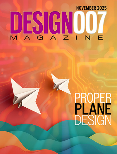
Designing Proper Planes
Without planes, designers would have to create thousands of traces to accomplish the same objectives. Power planes provide low impedance and stable power, and ground planes stabilize reference voltage, improve thermal performance, and help preclude EMI issues.

Power Integrity
Current power demands are increasing, especially with AI, 5G, and EV chips. This month, our experts share “watt’s up” with power integrity, from planning and layout through measurement and manufacturing.
- Articles
- Columns
- Links
- Media kit
||| MENU - design007 Magazine
EMA Launches Fun Valentine’s Day Contest for Electrical Engineers
February 10, 2016 | EMA Design AutomationEstimated reading time: 1 minute
With Valentine’s Day right around the corner, EMA Design Automation recently launched the Electrical Engineers Can Be Romantic Too contest. The contest began on February 8, 2016 and will continue until February 12, 2016 at 12 noon PST. The winner will be announced on February 12 at 3 pm PST.
In order to enter the contest, participants need to create a unique electrical engineering Valentine’s Day saying by either tweeting it to @EMA_EDA with the hashtag #EEsCanBeRomanticToo or e-mailing it to emamarketing@ema-eda.com with the subject line EEs Can Be Romantic Too. The winner will be announced February 13, 2016 and will receive the following:
- A custom-designed Valentine featuring their choice of saying
- An EMA messenger bag
- An EMA mug filled with chocolate
To complement this contest, EMA created free, engineering-themed, printable Valentine’s Day cards. EMA is releasing two sets of these great cards (which are sure to be a hit with any EE fan) are available on our blog at www.ema-eda.com/EMA-Blog.
For more information on the contest or to download the Valentine’s Day cards, click here.
About EMA Design Automation
EMA Design Automation is a trailblazer in product development solutions offering a complete range of EDA tools, product lifecycle management systems, services, training, and technical support. EMA is a Cadence® Channel Partner serving all of North America. EMA manufactures TimingDesigner®, CircuitSpace®, and a host of custom solutions to enhance the OrCAD products, and all are distributed through a worldwide network of value added resellers. EMA is a privately held corporation headquartered in Rochester, New York. Visit www.ema-eda.com.
Testimonial
"Your magazines are a great platform for people to exchange knowledge. Thank you for the work that you do."
Simon Khesin - Schmoll MaschinenSuggested Items
Pan-European Electronics Design Conference Returns Better Than Ever
12/11/2025 | I-Connect007 Editorial TeamFollowing a highly successful inaugural event, the Pan-European Electronics Design Conference (PEDC) returns, this time to Prague, Czech Republic, Jan. 21–22, 2026. In this Q&A, Peter Tranitz, the Global Electronics Association’s senior director of technology solutions, shares the value of attending PEDC, which aims to bring together PCB designers from across Europe to learn, network, and share their own knowledge.
Quilter Unveils World’s First Computer Designed by AI
12/10/2025 | BUSINESS WIREQuilter, the physics-driven AI for electronics design, announced the world’s first computer designed by artificial intelligence.
December 2025 Design007 Magazine: Designing Your Work and Your Life
12/08/2025 | I-Connect007 Editorial TeamEvery PCB design is a lesson in balance: speed vs. stability, density vs. clarity, performance vs. cost. What if we approached life with that same mindset? In the December issue of Design007 Magazine, we go beyond board design to show how designers, marketers, managers, and owners apply their professional skills to personal choices—and what it costs when that system is left to drift.
Siemens Partners with Certus Semiconductor to Advance AI-Driven Analog and IO/ESD Design
12/04/2025 | SiemensSiemens, a leading industrial technology company, announced that Certus Semiconductor has adopted Solido™ software for custom integrated circuit (IC) design to accelerate development of Input/output (IO) and Electrostatic Discharge (ESD) library solutions for the automotive, aerospace, mobile, consumer electronics industrial, AI and IoT applications.
Real Time with... productronica 2025: Polar on Understanding Material Libraries in Design
12/04/2025 | Real Time with...productronicaPete Starkey and Martyn Gaudion discuss the rapid updates in material libraries and the critical need for designers to grasp material properties. They highlight the role of suppliers and the importance of communication between designers and fabricators. Martyn focuses on the educational aspect of their services, aiming to connect design and manufacturing. The conversation underscores the significance of material knowledge in enhancing the design process through collaboration.


