-

- News
- Books
Featured Books
- smt007 Magazine
Latest Issues
Current Issue
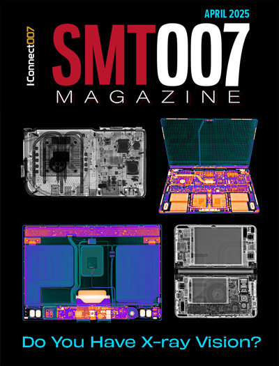
Do You Have X-ray Vision?
Has X-ray’s time finally come in electronics manufacturing? Join us in this issue of SMT007 Magazine, where we answer this question and others to bring more efficiency to your bottom line.

IPC APEX EXPO 2025: A Preview
It’s that time again. If you’re going to Anaheim for IPC APEX EXPO 2025, we’ll see you there. In the meantime, consider this issue of SMT007 Magazine to be your golden ticket to planning the show.

Technical Resources
Key industry organizations–all with knowledge sharing as a part of their mission–share their technical repositories in this issue of SMT007 Magazine. Where can you find information critical to your work? Odds are, right here.
- Articles
- Columns
Search Console
- Links
- Media kit
||| MENU - smt007 Magazine
Estimated reading time: 3 minutes
SMT Stencils 101: Root-cause Stencil Design, Part 2—Tombstones
In Part 1of this two-part column series, I discussed how one can address the challenge of solder balls before completing a build or starting production build. In Part 2, I will explore the second challenge we often hear about: tombstoning.
Tombstoning
Tombstoning defects on two-pin chips occur after reflow (Figure 1), but in many cases, can be corrected with stencil design. This process is very similar to performing a root-cause analysis to prevent solder balls in that first, the specific component drawing should be reviewed, and then the component outline created in Gerber. This Gerber representation of the component should be overlaid to the copper and mask layers to see how the part will sit in the solder paste after placement. At this stage, in many cases, one can see specific issues that may be causing the tombstoning to occur. When this overlay is reviewed, the outside edge of the component should sit very close to the midpoint of the stencil apertures.
When there are large areas extending beyond the component edge where solder paste is deposited, the possibility that one side becomes liquid before the other during the reflow process can cause tombstoning. Another cause of tombstoning can be that one side of the component land is tied to a ground plane, and the other side is not. The side not tied to a ground plane may heat up faster, causing solder paste to liquefy before the other land pad, resulting in tombstoning. This possibility should also be investigated if a larger-than-normal land pad is not present. Through many years of design and research in our lab, the reverse U-shape and reverse inverted homeplate aperture designs have been most successful in reducing or eliminating these tombstone issues (Figure 2).
These designs remove solder volume from the back-end of the package so that when the paste reflows, it wants to spread or pull toward the outside of the apertures holding the component down flat during reflow. Another way to describe what happens here is removing this paste on the outside of the component lowers the wetting force of the solder when it becomes liquid and helps prevent the component from tombstoning.
When designing the reverse U-shape aperture, one should pull the aperture toward the inside of the component so that the edge of the aperture is at the inside edge of the terminal or 2–3 mils inside the terminal edge. Please note that there should be 7.5 mils minimum between the inside edges of the stencil apertures for 0201 and larger chip components.
There are a lot of scenarios where the SMT pads on the board are not optimum. Sometimes, the pads are shifted too far apart, and other times, the pads are too long. In many cases, the solder paste brick needs to be pulled toward the inside of the component, removing paste from the outside of the component pads. Again, this places more paste under the part so that when it turns liquid, the paste spreads from under the component to the outside, holding the component down.
One final consideration is that when applying this design to chip components, the area ratio must be considered. When changing from a rectangle to this reverse U-shape or reverse inverted homeplate shape, more surface area is being added to the aperture walls. For example, a rectangular pad that is 13.8 mils square has an area ratio of 0.7, and the same aperture reduced by one mil per side with the reverse U-shape has an area ratio of 0.5. If the area ratio limit (i.e., 0.66) is exceeded, a standard reduction should be made, and a rounded square or rectangular aperture must be used.
Next Column
In my next column, I will discuss simple guidelines to reduce bridging at print and eliminate bridging after print for gull-wing leaded parts.
Greg Smith is manager of stencil technology at BlueRing Stencils.
More Columns from SMT Stencils 101
SMT Stencils 101: Root-cause Stencil Design, Part 3—Tearing Down BridgesSMT Stencils 101: Root-cause Stencil Design, Part 1—Solder Balls
SMT Stencils 101: What Are Industry-standard Stencil Designs?
Overcoming the Challenges of Miniaturization with New Stencil Technologies–Solder Paste Release, Pt. 2
Overcoming the Challenges of Miniaturization with New Stencil Technologies, Part 1: Solder Paste Release
A Brief History of Solder Stencil Manufacturing


