


 Learning with Leo: Drones—Meeting Demand Without Compromise
 Nolan’s Notes: Our Spotlight on North America
 Global Sourcing Spotlight: Building a Supply Chain That Bends, Not Breaks


Benefits of Soldering with Vacuum Profiles
April 8, 2015 | Helmut Oettl, Rehm Thermal SystemsEstimated reading time: 4 minutes
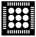
Requirements for void-free solder joints are continuously increasing in the field of electronics manufacturing (i.e., the reduction or elimination of cavities in the connection technology used between component connectors and connector pads). New challenges evolve on a daily basis due to the relentless introduction of new variants of so-called bottom-terminated components (BTCs), some of which are shown in Figure 1. Connector geometries alone are not decisive—numerous pitfalls are of greater significance. Incentives and several fundamentals will be elucidated in the following article.
The formation of solder joints is PCB manufacturing, and thus their quality, is influenced by an unmanageably large number of parameters, which are becoming increasingly difficult to master and control. A voids workgroup prepared the overview of factors shown in Figure 2, which provides an initial insight into the complexity of the problem. However, it only includes two factors that can be taken advantage of shortly before production of the affected PCBs in order to reduce or eliminate the formation of voids. These are the stencil and the layout of the aperture on the one hand, and the use of vacuum technology during the soldering process itself on the other hand. Vacuum soldering can even be used during the production processes as a sort of fire brigade when a short-term increase in the number of voids occurs. Thus, nothing stands in the way of using standard processes and standard profiles for series production; it’s possible to react flexibly to any fluctuation in the quality of purchased components, PCB surfaces and solder paste batches.
In addition to series production, PCBs can also be repaired in modern vacuum soldering systems like the CondensoX, in the event that excessively large voids have occurred during the initial soldering process in a conventional soldering system, which would otherwise have to be scrapped because they do not fulfill the criteria of the applicable IEC standards or IPC directives.
Vacuum is defined as follows in DIN 28400 (in agreement with ISO 3529-1):
“Vacuum is the state of a gas when the pressure of the gas, and thus the particle-number density, is lower within than it is outside of its container, or when the pressure of the gas is less than 300 mbar (i.e., lower than the smallest atmospheric pressure which occurs on the surface of the Earth.”)Page 1 of 2
Share on:


Testimonial
"Our marketing partnership with I-Connect007 is already delivering. Just a day after our press release went live, we received a direct inquiry about our updated products!"
Rachael Temple - AlltematedSuggested Items
AQUANOX A4727 and A4625 Lead KYZEN Offerings at SMTA Oregon Expo and Tech Forum
05/06/2026 | KYZENKYZEN, the global leader in innovative environmentally responsible cleaning chemistries, will exhibit at the SMTA Oregon Expo and Tech Forum scheduled to take place Thursday, May 19 at the Wingspan Event and Conference Center in Hillsboro, Oregon.
Connect the Dots: Designing for the Future of Manufacturing Reality—Surface Finish
05/07/2026 | Matt Stevenson -- Column: Connect the DotsWhen designing the complex boards that many electronic devices require to operate, designers should consider manufacturability at every step. This is my last article focused on designing for the always-evolving manufacturing reality. Choosing the right surface finish has always been important. If you are creating intricate designs with a wide variety of components, like for an ultra-high density interconnect (UHDI) board, surface finish is a critical last step.
Indium to Showcase High-Performance AI Application Solutions at SEMICON SEA 2026
05/01/2026 | Indium CorporationAs a leading provider of advanced materials solutions for today’s demanding AI applications, Indium Corporation® will feature its high-reliability product portfolio at SEMICON SEA 2026, May 5-7, in Kuala Lumpur, Malaysia.
ACCM Unveils Negative and Near-zero CTE Materials for Large-Format AI Chips
04/21/2026 | Advanced Chip and Circuit MaterialsAdvanced Chip and Circuit Materials, Inc. (ACCM) has launched two new materials: Celeritas HM50, with a negative coefficient of thermal expansion (CTE) of -8 ppm/°C to offset the positive CTE and expansion of copper with temperature on circuit boards, and Celeritas HM001, with near-zero CTE and the low-loss performance needed for high-speed signal layers to 224 Gb/s and faster in artificial intelligence (AI) circuits.
SMTA Ultra HDI Symposium, Day 2: Fragile Supply Chains, Fierce Innovation
04/14/2026 | Marcy LaRont, I-Connect007The Arizona weather yielded another beautiful day as we gathered for the second day of SMTA’s annual UHDI symposium. After the first full day discussing the role of AI in business and the how-tos of implementation, Avondale Mayor Mike Pineda kicked off day two, proud to showcase his city and to declare its important place in the continued development of the West Valley, an increasingly important area for tech and manufacturing.