-

- News
- Books
Featured Books
- design007 Magazine
Latest Issues
Current Issue
All About That Route
Most designers favor manual routing, but today's interactive autorouters may be changing designers' minds by allowing users more direct control. In this issue, our expert contributors discuss a variety of manual and autorouting strategies.

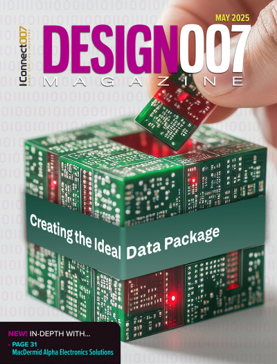
Creating the Ideal Data Package
Why is it so difficult to create the ideal data package? Many of these simple errors can be alleviated by paying attention to detail—and knowing what issues to look out for. So, this month, our experts weigh in on the best practices for creating the ideal design data package for your design.

Designing Through the Noise
Our experts discuss the constantly evolving world of RF design, including the many tradeoffs, material considerations, and design tips and techniques that designers and design engineers need to know to succeed in this high-frequency realm.
- Articles
- Columns
- Links
- Media kit
||| MENU - design007 Magazine
Ultra HDI Primer
October 13, 2022 | I-Connect007 Editorial TeamEstimated reading time: 3 minutes
We recently spoke with Herb Snogren, an industry veteran and consultant with Summit Interconnect tasked with leading the company’s ultra HDI efforts. Herb is co-chair of the IPC ultra HDI subcommittee, IPC D-33-AP. In this interview, Herb discusses the current state of UHDI, how designers and fabricators can get started working in this new frontier, and why the U.S. must invest in UHDI technology now to counteract Asia’s near dominance of the UHDI segment, which has left some of our critical industries vulnerable to supply chain disruptions.
Andy Shaughnessy: Herb, almost everyone I talk to about this topic asks me, "What is the definition of ultra HDI?” What’s the manufacturable limit?
Herb Snogren: We've developed an IPC subcommittee, IPC D-33-AP. Jan Pedersen of NCAB Group is my co-chair, and we’ve defined ultra HDI as printed circuit boards that have line widths and spaces below 50 microns, and microvias at 75 microns and below in diameter. We came up with that delineation because of IPC-2226, which lists product attributes with producibility levels A, B, and C. Level C is the lowest producibility level and that stops at 50-micron lines and spaces.
Shaughnessy: Tell us about the committee’s efforts.
Snogren: What’s important to understand is that circuit boards are following the path of packaging substrates. We now have the term SLP (substrate-like PCB) because printed circuit boards, at least in Asia for small form-factor products, are being produced with manufacturing techniques similar to IC substrates. IC substrates now have line widths and spaces down to 6 and 8 microns, and that's where we're going. When you look at some of the Apple and Samsung products, they're in the 20- to 25-micron line and space range in high volumes.
Shaughnessy: For years, we’ve been hearing that the convergence of IC and PCB processes was on the horizon. It seems like we’re finally there now.
Snogren: We are. Historically, IC substrates were made with semi-additive or modified semi-additive processing, and now printed circuit boards are being made with semi-additive and modified semi-additive processing. It is really happening.
Shaughnessy: Is Asia the center of ultra HDI?
Snogren: Yes. It really started with Apple working with their suppliers in Asia to get their line widths and spaces down. They did it in a big way, but because of that, other companies are taking advantage of the capability that’s been established. There are companies in other parts of the world that can do that. There may be one or two in Israel and Europe, but more than 95% of the volume is being done in Asia, with most of it in China.
Shaughnessy: What segments are driving the development of ultra HDI?
Snogren: It’s anything that has a small form factor. It started with the cellphone, just trying to pack more capability into a small space. You see it in medical devices that need to be small, such as in-ear devices or hearing aids. We need to do implantable devices that must be small and innocuous. With heterogeneous integration and cramming more transistors into a square inch through heterogeneous packaging, there are more I/Os on the device. The I/O density increases, so your pitch decreases, and that’s driving this as well.
Shaughnessy: Are design engineers from the PCB side studying IC laminate design processes, and vice versa?
Snogren: Product designers need to understand there is a manufacturing process capable of producing these finer features, and they can employ those in their products to reduce the size of the product or reduce layer count. The problem is you can’t get it in the United States, so if they design it, they don’t have a place to buy it here. You must go to Asia. Right now, companies are trying to develop it. Averatek has some licensees who can do this. Winonics (Additive Circuits Technologies) has a similar technology it is developing. But I don’t know if anyone is doing anything in a meaningful way or volume. Certainly not in any kind of volume at this point.
To read this entire conversation, which appeared in the October 2022 issue of Design007 Magazine, click here.
Suggested Items
Intervala Hosts Employee Car and Motorcycle Show, Benefit Nonprofits
08/27/2024 | IntervalaIntervala hosted an employee car and motorcycle show, aptly named the Vala-Cruise and it was a roaring success! Employees had the chance to show off their prized wheels, and it was incredible to see the variety and passion on display.
KIC Honored with IPC Recognition for 25 Years of Membership and Contributions to Electronics Manufacturing Industry
06/24/2024 | KICKIC, a renowned pioneer in thermal process and temperature measurement solutions for electronics manufacturing, is proud to announce that it has been recognized by IPC for 25 years of membership and significant contributions to electronics manufacturing.
Boeing Starliner Spacecraft Completes Successful Crewed Docking with International Space Station
06/07/2024 | BoeingNASA astronauts Barry "Butch" Wilmore and Sunita "Suni" Williams successfully docked Boeing's Starliner spacecraft to the International Space Station (ISS), about 26 hours after launching from Cape Canaveral Space Force Station.
KIC’s Miles Moreau to Present Profiling Basics and Best Practices at SMTA Wisconsin Chapter PCBA Profile Workshop
01/25/2024 | KICKIC, a renowned pioneer in thermal process and temperature measurement solutions for electronics manufacturing, announces that Miles Moreau, General Manager, will be a featured speaker at the SMTA Wisconsin Chapter In-Person PCBA Profile Workshop.
The Drive Toward UHDI and Substrates
09/20/2023 | I-Connect007 Editorial TeamPanasonic’s Darren Hitchcock spoke with the I-Connect007 Editorial Team on the complexities of moving toward ultra HDI manufacturing. As we learn in this conversation, the number of shifting constraints relative to traditional PCB fabrication is quite large and can sometimes conflict with each other.


