


 Beyond Design: Slaying Signal Integrity Villains
 Elementary Mr. Watson: Running the Signal Gauntlet
 The Shaughnessy Report: Winning the Signal Integrity Battle


IPC Training Course on PCB Design for Printed and Wearable Devices
May 27, 2022 | IPCEstimated reading time: 1 minute
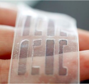
IPC will be holding a training course on PCB design for printed and wearable devices. The course will be held every Mondays and Wednesdays, 6:30 p.m. to 8:30 p.m., starting from June 6 to July 18, 2022.
This course aims to provide the skills necessary to create designs for printed electronics and wearable technologies in accordance with IPC standards. Taught by an IPC-certified industry expert with more than 25 years of experience in the field, the six-week program utilizes interactive webinars, on-demand recorded class sessions, job-specific exercises, and projects to facilitate mastery of the key concepts required by circuit board designers.
The program is designed to provide circuit board designers with a balanced foundation of theoretical knowledge and practical skills in printed circuit board design. Upon completion, participants will be able to design boards for printed electronics and wearables; understand the trade-offs in materials used in these applications; define a board stack-up with structures that meet the needs of these designs and mitigate signal integrity issues for these designs.
Attendees will also be able to define the effects of mechanical retention needs for these applications; implement component footprint and packaging methodologies; mitigate thermal effects; and employ the documentation requirements for these designs.
For more information visit IPC’s website.
Share on:


Testimonial
"Our marketing partnership with I-Connect007 is already delivering. Just a day after our press release went live, we received a direct inquiry about our updated products!"
Rachael Temple - AlltematedSuggested Items
Electrodeposited Copper Foils Market to Grow by $11.7 Billion Over 2025-2032
09/18/2025 | Globe NewswireThe global electrodeposited copper foils market is poised for dynamic growth, driven by the rising adoption in advanced electronics and renewable energy storage solutions.
Breakthrough in Non-Contact Solder Removal Earns Kurtz Ersa 2025 Mexico Technology Award at SMTA Guadalajara
09/18/2025 | Kurtz Ersa Inc.Kurtz Ersa Inc., a leading supplier of electronics production equipment, is proud to announce that it has been awarded a 2025 Mexico Technology Award in the category of Rework & Repair for its HR 600P Automatic Rework System.
A.R.T. Invests in Latest Equipment to Further Enhance Electronics Training Facilities
09/17/2025 | A.R.T. Ltd.Advanced Rework Technology Ltd. (A.R.T.), a leading independent IPC-accredited training provider, has announced a series of new equipment investments at its state-of-the-art training centre.
Richardson Electronics Appoints Daniel Albers to Drive Made-in-USA Contract Manufacturing Expansion
09/17/2025 | Globe NewswireRichardson Electronics, Ltd., a global provider of engineered solutions for the green energy, power management, and custom display markets, announced the appointment of Daniel Albers to spearhead business development for its expanded, Made-in-USA contract manufacturing efforts.
STMicroelectronics to Advance Next-generation Chip Manufacturing Technology with New PLP Pilot Line in Tours, France
09/17/2025 | STMicroelectronicsSTMicroelectronics, a global semiconductor leader serving customers across the spectrum of electronics applications, today announced new details regarding the development of the next generations of Panel-Level Packaging (PLP) technology through a pilot line in its Tours site, France, which is expected to be operational in Q3 2026.