


 Connect the Dots: Designing for the Future of Manufacturing Reality—Solder Mask and Legend
 Target Condition: An Exploration of Flooding PCB Layers
 Happy’s Tech Talk #47: Automation for Complex Multilayer Fabrication Stackups


Polar Talks Impedance Control and Insertion Loss Testing
June 9, 2015 | Dan Feinberg, FeinLine Associates, Inc.Estimated reading time: 5 minutes
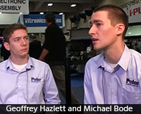
During IPC APEX EXPO, I sat down with Polar Instruments product specialists Michael Bode and Geoffrey Hazlett to talk about the company and its products and solutions. We also discussed some of the signal integrity technologies being enabled by the company, including controlled impedance and insertion loss testing.
Dan Feinberg: I’m speaking with Michael Bode and Geoffrey Hazlet, product specialists with Polar Instruments. Gentlemen, welcome.
Michael Bode: Thank you.
Geoffrey Hazlet: Thank you.
Dan Feinberg: Welcome to San Diego. I think you're just about to miss the rain. Gentlemen, you're with Polar Instruments; tell me about Polar.
Bode: Sure. Polar's been around for about 40 years, originally started in the United Kingdom on a small island called Guernsey. We are well known in the PCB fabrication industry and in the design industry. We have a variety of tools; the most well-known would be our field solvers for controlled impedance modeling, insertion loss modeling, PCB design. We also have a stackup design tool, as well as a variety of corporate products for actually testing controlled impedance and testing insertion loss.
Feinberg: That brings up a question. Controlled impedance: What are the advantages of controlled impedance? It's not being used by everyone, but there are obviously some advantages. Why would someone want to do impedance control or calibration?
Bode: It all depends on what you're trying to make. For some boards, the traces, the transmission lines, must be exactly the way that they're specified by the designer, which makes it critical for fabricators to build exactly what they think they're building. With the Polar suite, we can actually help them do that design work, and then verify, "Hey, did you build what you think you built?" For some of your designs, that's going to be really important.
Feinberg: I get the impression that everyone doesn't build what they think they’ve built.
Bode: Yeah, that does happen.
Feinberg: Geoffrey, where do you see the technology that your company focuses on heading? What do you see coming about in the near future?
Hazlet: Just like we were talking about controlled impedance, and that's sort of a ubiquitous term in our industry. Now that a lot of PCB fabricators are already familiar with at least the concept of controlled impedance traces on their boards, designers are familiar with it. What's coming out now, and has been slowly rolling out, is more insertion loss, characterization, and requirements that the OEMs are putting on fabricators, saying, "Great, you've got the right controlled impedance for me now, but I also need certain insertion loss characteristics."
So, if the impedance is off, the signal's not going to get through. Now, the impedance is on, but the signal's still not getting through because of the loss of the materials in the copper. Designers, as well as fabricators, need to work together to make sure that the signal is still getting through. As part of that, we've moved in the direction of also providing insertion loss testing tools, implementing IPC methods for SPP and SET2DIL [insertion loss test methods].
Feinberg: How do you see that as compared to what was going on, let's say, 10 years ago?
Hazlet: Ten years ago and 15 years ago, the industry still wasn't really jumping onto controlled impedance testing. It was still an early thing for the industry, so some people were sitting back. Some fab shops still don't provide that service, whereas if you look at the large fabricators out there, they all perform or have the capability to perform impedance testing. A lot of them are already getting on board as early adopters of insertion loss testing. We're seeing that it's still in the early adopter phase, but it's quickly shifting over. Asian fabricators are buying up test systems very rapidly now, we didn't even see that two years ago. Now, it's suddenly kind of over the cliff, if you will.
Feinberg: You guys think that this is something that will become mainstream, perhaps, in five years?
Hazlet: Yeah. I think it'll be just another testing method that OEMs will require their PCB fabricators to perform.
Feinberg: It kind of goes along with some of the IPC specifications, specs and so forth.
Hazlet: Yeah, it does.
Feinberg: Michael, tell me about some of the new products that you’re showing at IPC APEX EXPO 2015, and the new technologies that you're talking about this year.
Bode: One of the major products that we're showing here today, which is new for us is a new model of our impedance tester. It's called the CITS 880S, that's the controlled impedance test system. This model of the tester employs a new measurement technique which is called launch point extrapolation. This is important for measuring impedance of lossy lines, which have a significant series resistance component. What that means is that the old methods of measuring impedance didn't really do a good job of measuring the impedance of the lossy lines. Which this new technique what we're able to do is calculate what's the instantaneous impedance at the beginning of the trace before those resistance components have taken effect. That's something that IPC has been working to validate that particular technique, I think that they're almost through with the approval process with that.
Hazlet: You're actually working with them to help that process right?
Bode: Yeah, that's right.
Feinberg: Gentlemen, anything else that you'd like to add? Do you see anything else with regard to new technologies and products that you'll be coming out with that you could talk about?
Bode: There is the topic of flex design, we were just chatting beforehand about how that's becoming more critical for some designs. We're seeing a lot more people saying, "Hey, we want to do this flex-rigid-flex design." Especially with controlled impedance, that's the direction that we see our new products going and just more capability with that.
Feinberg: Especially with all of the handheld devices and all of the portable devices, flex circuitry, flex assembly is becoming much, much larger.
Hazlet: Almost every time I ask someone who's coming up and talking about stack up design. I ask them, "Do you do any HDI or flex or rigid-flex builds?" Without a doubt, they say either yes, or, "Not yet, but I will probably in the next year or so."
Feinberg: You know it's coming. Well, gentlemen, thank you very much for your time.
Share on:


Testimonial
"Advertising in PCB007 Magazine has been a great way to showcase our bare board testers to the right audience. The I-Connect007 team makes the process smooth and professional. We’re proud to be featured in such a trusted publication."
Klaus Koziol - atgSuggested Items
Nortech Systems Launches Power over Fiber Technology Platform for EMI-Sensitive Applications
04/08/2026 | Globe NewswireNortech Systems Incorporated, a leading provider of design and manufacturing solutions for complex electromedical devices and electromechanical systems, has announced the launch of its Power over Fiber technology platform.
Flexible Thinking: Designing Flex Circuits for Dynamic Reliability
04/09/2026 | Joe Fjelstad -- Column: Flexible ThinkingFlex circuits flex. No surprises there. However, they are also very commonly designed into products because they are thin and offer consistent thickness and dielectric properties, attributes highly prized by present-day product designers of personal electronics. This would include smartphones and, increasingly, wearable electronics for medical monitoring and even fashion.
Understanding Tolerances in Flexible Circuit Design
04/01/2026 | Chris Clark, Flexible Circuit TechnologiesThe challenge with cumulative tolerances is meeting the dimensional requirements for items dimensioned on a drawing or specification for a flexible or rigid-flex circuit. It is critical to understand the fabrication processes and how features are defined when creating your tolerance requirements.
Target Condition: An Exploration of Flooding PCB Layers
04/02/2026 | Kelly Dack -- Column: Target ConditionThe concept of flooding PCB layers with copper has been around for so long, you’d think we’d have it mastered. We haven’t. (Oh, and by “we,” I mean design engineers and the software tools we depend on.) Years ago, PCB artwork was created by hand using light tables, with tape applied to Mylar. Signals were slow, traces were relatively wide, and high-current paths were simply “beefed up” with wider copper. Signal integrity wasn’t yet a driving concern. Today, solid return paths are fundamental to robust design. We understand the importance of continuous reference planes for signal integrity and EMI control.
New, Greener Solutions for Etch: Novel Copper Extraction
03/30/2026 | Richard Nichols, GreenSource Engineering“Novel” is a typical marketing phrase that implies new and unique, but often “novel” actually means an established technology being applied to a new field or application. This, in turn, is often driven by newly relevant external motivation. GreenSource has been working on just such a solution: novel copper extraction, offering a better and greener alternative to traditional LLE control systems for cupric chloride etch.