


 Dan’s Biz Bookshelf: ‘Dream First Details Later
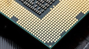
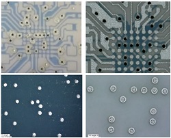
 Happy’s Tech Talk #40: Factors in PTH Reliability—Hole Voids
 Facing the Future: Time for Real Talk, Early and Often, Between Design and Fabrication


Latest Articles
Putting Green Into a Brownfield Facility

George Milad, national accounts manager for technology at Uyemura, talks about what is driving change in the wet process marketplace and how chemistries must fit into next-generation product design while also meeting new environmental requirements.
The Advantages of Non-sludge Acid Copper Products

Mike Wood, technical director with Cerambus Asia Pacific, discusses the acid copper product from Cerambus Technology Inc. that doesn't generate sludge during the plating process and operates at higher production output by using higher current density. He talks about why this is important for the state of the vertical continuous plating (VCP) market in Asia, and the trends he’s seeing in that space.
The State of Plating

Increasingly, PCB design technology utilises buried and blind via holes and plated via fill is also becoming more and more common. The buried and blind holes mean that the loading on the plating equipment is multiplied by the number of different inner layer connections. The same technology means that equipment needs to deal with thinner and thinner materials.
Meet Mike Hill, I-Connect007 Columnist

Mike Hill has been in the PWB fabrication industry for over 40 years. Throughout his career, he has been a member of IPC and participated in specification writing for both IPC and the military. Within IPC, he has received the President's Award, General Chairmanship, Committee Chairmanship, and many other recognitions. In his columns, Mike will help you better understand the requirements and how-to's for MIL-PRF-31032 certification for PWB fabrication.
Pollution Prevention Techniques: Rinse Water Reduction

There are five general categories of common techniques for pollution prevention in a PCB fabrication facility: new processes to replace sources of pollution; extend the bath’s life; rinse water reduction; dragout reduction; and ventilation reduction. While this list is not all-inclusive, it provides an overview of the types of technologies used around the world that are important to consider. This article, examines rinse water reduction.
Words of Advice: Obstacles to Solid Data Hand-off

In a recent survey, we asked the following question: What are the biggest obstacles you face in getting your design to the fabricator? Here are a few of the answers, edited slightly for clarity.
SAP Utilizing Very Uniform Ultrathin Copper

The demand for miniaturization and higher density electronic products has continued steadily for years, and this trend is expected to continue, according to various semiconductor technology and applications roadmaps. The semiconductor miniaturization brings significant economic and technical benefits and the semiconductor scale factor becomes the master for the associated package and PCB design.
Innovative Electroplating Processes for IC Substrates
The decreasing chip scales and smaller line/spacing distances have created unique challenges for both the PCB industry and the semiconductor industry. This paper discusses innovative additive packages for direct-current copper electroplating specifically for IC substrates, which offer better trace profile and deliver via fill and through-hole plating. It also describes two electrolytic copper plating processes, the selection of which could be based on the via size and the dimple requirements of the application.
Vertical Conductive Structures, Part 3: Design Tool Techniques
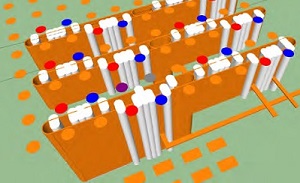
New vertical conductive structure (VeCS) technology can reduce layer count and improve signal integrity without the need for sequential technologies. VeCS is different than traditional through-hole vias, microvias, and ELIC designs, which are more expensive and require a high number of laminations, drilling, and plating cycles to build up a reasonable number of layers.
Words of Advice: Your Company’s Design Process
In a recent survey, we asked PCB designers to describe their company’s design process: Is it a rigid workflow they follow to the letter, or a process that allows for their individual techniques? Of course, the comments were illustrative.
Nano Dimension Details New DragonFly LDM
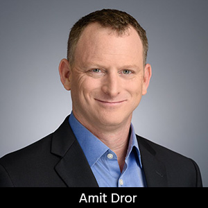
Dan Feinberg talks with Nano Dimension CEO Amit Dror about the new DragonFly LDM 3D printer technology announced by the Israeli company on July 24, 2019, aimed at increasing machine uptime and moving forward from prototyping to higher production volumes.
Bill Brooks on Teaching PCB Design at Palomar College

Bill Brooks of Nordson ASYMTEK is a long-time PCB designer and one of the first people to teach PCB design courses in a college setting. He recently spoke with the I-Connect007 editorial team about his history in design and his time as a PCB design instructor, the curriculum he developed and taught, and various techniques that might be enacted today to better educate the designers of tomorrow.
Solder Mask Curing: UV Bump Overview

Ultraviolet (UV) bump, also called UV cure, is a processing step in which the solder mask pattern is irradiated with ultraviolet and infrared light. This step is performed with special equipment that is built as a continuous flow system, which consists of a conveyor belt and tubular UV lamps mounted above and below the belt. Read on to find out more about this process.
There’s An Art to Plating

There's definitely an art to plating. Start with a generally planar substrate, then alternately put stuff on and take things off. Continue this in subtle variations until what you have is the stuff you want, where you want.
Words of Advice: Drawbacks to Your PCB Data Format?
In a recent survey, we asked the following question: What is the biggest drawback to your current PCB data format? Here are a few of the answers, edited slightly for clarity.
Development of Flexible Hybrid Electronics
This article will present a hybrid manufacturing process to manufacture FHE systems with a two-layer interconnect structure utilizing screen printing of silver conductive ink, filled microvias to connect ink traces at the different layers, and use of the traditional reflow process to attach the semiconductor chips to the printed substrates.
Names to Know: Up and Comers in U.S. Congress

When major news occurs in the U.S. Congress, you usually hear the names of top congressional leaders such as House Speaker Nancy Pelosi (D-CA) or Senate Majority Leader Mitch McConnell (R-KY).
Meet Chris Mitchell, I-Connect007 Columnist

Chris Mitchell is vice president for global government affairs at IPC—Association Connecting Electronics Industries—where he is responsible for development and implementation of the organization’s global advocacy efforts and public policy agenda with a focus on electronics industry business improvement, environment, health and safety, and defense initiatives.
Words of Advice: Planning a New Design
In a recent survey, we asked the following question: What do you think is the most important thing a designer should remember when planning a new PCB design? Here are a few of the answers, edited slightly for clarity.
The Impact of Inductance on Impedance of Decoupling Capacitors

This article discusses the impact of interconnection inductance on the impedance of the decoupling capacitor, which influences the power integrity of the PCB. The investigation is performed with 3DEM simulation by varying the trace length and height of stitching vias that connect the decoupling capacitor across the power rail and ground.
Altium Designer 19.0 Features Printed Electronics Design Functions

The newest version of Altium Designer—revision 19.0—includes functionality for designing printed electronic circuits. We wanted to get the scoop on Altium’s PEC tools, so we asked Nikolay Ponomarenko, Altium’s director of product management, to give us a tour of the new functions.
IPC Reliability Forum Wrap-up With Brook Sandy-Smith

I attended the recent IPC High-Reliability Forum and Microvia Summit in Baltimore, Maryland. The speakers and panelists focused on a variety of topics, but one issue that kept popping up was the failure of some microvias on military and aerospace PCBs. Fortunately, some smart technologists are focusing on determining the cause of these via failures. I asked Brook Sandy-Smith, IPC’s technical education program manager, to give us a quick wrap-up of this event.
Denny Fritz: The Difference Between Quality and Reliability

I recently spoke with industry veteran (and I-Connect007 columnist) Denny Fritz about the relationship between quality and reliability—two terms that are unequal but often used interchangeably. We also discuss the current state of lead-free solders in the U.S. military and defense market as well as the microvia reliability issues Denny focused on at IPC’s High-Reliability Forum and Microvia Summit in Baltimore, Maryland.
IPC High-reliability Forum and Microvia Summit Review, Part II

The Microvia Summit on May 16 was a special feature of the 2019 event in Baltimore, since microvia challenges and reliability issues have become of great concern to the PCB manufacturing industry. It provided updates on the work of members of the IPC V-TSL-MVIA Weak Interface Microvia Failures Technology Solutions Subcommittee and opportunities to learn about latest developments in methods to reveal and explain the presence of latent defects, identify causes and cures, and be able to consistently and confidently supply reliable products.
Mentor Tools: Optimized for Flex and Rigid-flex Design

With the launch of the new Flex007 section in Design007 Magazine, we asked David Wiens, product marketing manager with Mentor, a Siemens Business, to tell us about their tools’ flex and rigid-flex design capabilities. As David explains, today’s higher-end design software tools are optimized for flex design, making workarounds a thing of the past.
Copyright © I-Connect007 | IPC Publishing Group Inc. All rights reserved.
Log in