


 Connect the Dots: Designing for the Future of Manufacturing Reality—Solder Mask and Legend
 Target Condition: An Exploration of Flooding PCB Layers
 Happy’s Tech Talk #47: Automation for Complex Multilayer Fabrication Stackups


Book Excerpt: 'An Introduction to The Printed Circuit Designer’s Guide to… Stackups'
October 6, 2022 | I-Connect007Estimated reading time: 1 minute
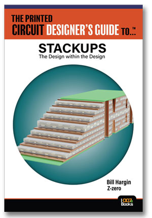
The Printed Circuit Designer’s Guide to... Stackups—The Design within the Design is written by Bill Hargin
Introduction: Mechanical Versus Electrical Worlds
Another book about stackups?
If you’re asking this question, I’d like to know the book you’re thinking of, as I was looking for it a few years back. I have a pretty good PCB signal integrity (SI) library, and I’ve only found one chapter on stackup design so far.
Whenever I talk in person with SI consultants—people who do SI consulting for a living—I ask them, “Of the smoke-jumping projects you’ve been brought in for where there were serious SI problems, how many of those projects have stackup issues?” So far, the only answer I’ve gotten back is, “100 percent.”
The difference between a high-speed PCB design that can be built, and a design that should be built, depends upon the backbone of the design itself: the stackup. The stackup touches every single high-speed signal and yet has had surprisingly little written about it.
In my work, quite a number of PCB stackups cross my desk, and depending on who or what tools were involved in a given design, there are manufacturing parameters that affect both impedance and signal loss that design teams can improve upon.
This book is by no means the last word on the subject, but rather a place to kick off a broader discussion about stackup planning and material selection, to reach the understanding of what I call “the design within the design.”
Share on:


Testimonial
"In a year when every marketing dollar mattered, I chose to keep I-Connect007 in our 2025 plan. Their commitment to high-quality, insightful content aligns with Koh Young’s values and helps readers navigate a changing industry. "
Brent Fischthal - Koh YoungSuggested Items
Teradyne Acquires TestInsight, Accelerating Time to Market for AI and Data Center Devices
04/16/2026 | BUSINESS WIRETeradyne, Inc., a leading provider of automated test equipment (ATE) and advanced robotics, announced it has acquired TestInsight, a leading provider of semiconductor test development, validation, and conversion software widely used across the industry.
Cadence, Google Scale AI Chip Design with ChipStack on Google Cloud
04/16/2026 | Cadence Design SystemsCadence, an industry leader in AI-driven computational software for semiconductor and system design, announced a strategic collaboration with Google to optimize the Cadence® ChipStack™ AI Super Agent with Gemini on Google Cloud.
ESD Alliance Reports Electronic System Design Industry Posts $5.5 Billion in Revenue in Q4 2025
04/15/2026 | SEMIElectronic System Design (ESD) industry revenue increased 10.3% to $5,466.3 million in the fourth quarter of 2025 from the $4,955.2 million registered in the fourth quarter of 2024, the ESD Alliance, a SEMI Technology Community, announced today in its latest Electronic Design Market Data (EDMD) report.
April Issue of I-Connect007 Magazine: Beyond the Rulebook
04/14/2026 | I-Connect007 Editorial TeamIn this month’s I-Connect007 Magazine, we asked PCB designers, fabricators, and suppliers what it really means to operate without a rulebook. Their perspectives vary, especially between seasoned designers and experienced fabricators, but a common thread emerges: progress depends on pushing boundaries and finding a way forward, even when the path isn’t clear. In many ways, this mindset has always been part of what we do, whether we’ve called it that or not.
Powering the Future: Why Thermal Management Defines the Future of Electronics
04/15/2026 | Brian Buyea -- Column: Powering the FutureEvery leap forward in electronics comes with a familiar consequence: heat. Whether it’s a power module driving an electric vehicle, a laser diode used in surgery, or a 5G amplifier operating in orbit, higher performance inevitably means higher temperatures. While engineers celebrate breakthroughs in speed, density, and power, none of those specifications matter if the system can’t keep cool long enough to perform reliably.