


 It’s Only Common Sense: Creativity Is Noisy, Messy, and So Worth It
 Dan’s Biz Bookshelf: ‘The Soul of a New Machine’
 The Chemical Connection: Back to Basic Cupric Chloride Etching


EPTE Newsletter: Monocoque Printed Circuits, Part 4
Based on past columns where I explored the basic concept of monocoque printed circuits, I received many inquiries and questions about this new circuit technology. Circuit engineers and designers need a feasible 3D wiring method to use as an alternative technology in flexible circuits. A lot of money is budgeted for complicated wiring in the limited spaces of smartphones, digital cameras, and other mobile devices.
Electronic circuits are formed in plastic framing or housing—an idea created by circuit engineers years ago called molded interconnect device (MID). Several processes were used to try and build 3D wiring on plastic parts, but these attempts were unsuccessful. The processes were too complicated, and manufacturers could not justify using any of them due to the negligible yields.
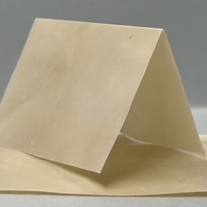
Columbus’ egg refers to an idea that seems simple after the fact (Google it for the reference: “Egg of Columbus”). A thick-film circuits engineer was watching the vacuum forming process from a PET sheet and wondered if the PET sheet could have a circuit on the surface. Thermal forming is a very common process to create transparent packages for general goods, and Polymer thick-film circuits are widely used to place electronic circuits on PET films.
The process is very simple, as illustrated in Figure 1. The thick-film circuits are first screen-printed on thermoplastic sheets and formed in the die at the appropriate temperature.
Previously, MID manufacturers were not very successful in creating electronic circuits on 3D formed parts. Thanks to the film circuits engineer mentioned earlier, various circuits can be created on flat plastic sheets, which are then formed in a heated die set. Some mechanical stresses show on the corners of the formed parts, but several newly developed silver inks can minimize the distortions of the printed conductors. This simple process leaves us with reliable 3D circuits and bountiful yield.
We use a traditional assembling process. Traditional soldering is not available, but we developed an SMT process using conductive glue. Most of the connectors designed for rigid circuit boards and flex circuits are available with just a few minor modifications.
The technology is relatively new and does not have a long history in actual applications. The trials will make the monocoque circuit technology universally accepted, especially for large volume consumer products once trials are underway. I am very optimistic about this technology.
Editor’s note: Read Part 1, Part 2, and Part 3 on monocoque printed circuits.
Headlines
1. TPCA (PCB industry organization in Taiwan) 6/17
May PCB shipment unexpectedly declined 4.6% from April; rigid boards declined 1.3%, and flex circuits declined 13.5% from April, but they keep positive growths from the same month of the previous year.
2. Gifu University (Japan) 6/22
Co-developed a tiny antenna for tera-Hz wireless telecommunication targeting beyond 5G and 6G (size: 1.36 x 1.36 x 1.72 mm).
3. Taiyo Yuden (component supplier in Japan) 7/1
Rolled out a new series of MCLL capable of 150°C, assuming automobile use (size: 1,005~3,225, capacity: ~0.1 micro F).
4. Rohm (device manufacturer in Japan) 6/17
Developed a new small-size blue-green color LED with high reliability (wavelength: 505 nm, size: 1.6 x 0.8 mm).
5. Osaka Prefecture University (Japan)
Succeeded to develop a new cathode material for the all-solid-state secondary battery. The new material enlarges the battery capacity remarkably.
6. SCREEN (equipment manufacturer in Japan) 6/29
Rolled out a new spin processor SP-2100 for 8” wafer or smaller. The company expects 8” or smaller wafers could be major in IoT and 5G markets.
7. Canon (electronics company in Japan) 6/30
Developed a new single-photon avalanche diode (SPAD) image sensor with one million pixels for 3D cameras.
8. Kyoto Semiconductor (semiconductor manufacturer in Japan) 7/1
Developed a new InGaAs base photo diode capable of modulation for a 40-GHz band, considering over 400 Gbit/sec transmission (size: 0.6 x 0.48 x 0.25 mm).
9. Kioxia (semiconductor manufacturer in Japan) 7/1
Completed the M&A of SSD business from LITE-ON in Taiwan. The company will continue to use the current brand.
Dominique K. Numakura is the managing director of DKN Research LLC. Contact haverhill@dknreseach.com for further information and news.


