-

- News
- Books
Featured Books
- design007 Magazine
Latest Issues
Current Issue
Signal Integrity
If you don’t have signal integrity problems now, you will eventually. This month, our expert contributors share a variety of SI techniques that can help designers avoid ground bounce, crosstalk, parasitic issues, and much more.

Proper Floor Planning
Floor planning decisions can make or break performance, manufacturability, and timelines. This month’s contributors weigh in with their best practices for proper floor planning and specific strategies to get it right.

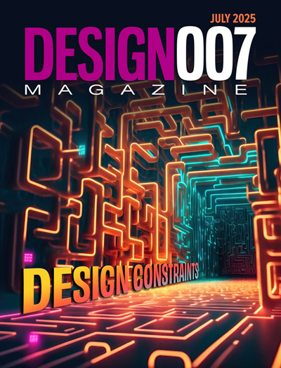
Showing Some Constraint
A strong design constraint strategy carefully balances a wide range of electrical and manufacturing trade-offs. This month, we explore the key requirements, common challenges, and best practices behind building an effective constraint strategy.
- Articles
- Columns
- Links
- Media kit
||| MENU - design007 Magazine
From Silicon to Systems
September 10, 2024 | Andy Shaughnessy, Design007 MagazineEstimated reading time: 2 minutes
For the past few years, IPC has been championing the term “silicon to systems.” More than a buzzword, it has become a slogan—and even a kind of roadmap—for the organization. The term comes in especially handy when IPC is advocating for this industry in Washington, D.C., often addressing politicians who have little understanding of electronics technology.
But what does silicon to systems mean to PCB designers? We asked this and more of a trio of IPC staffers: CTO Matt Kelly, Chief Strategist for Advanced Packaging Devan Iyer, and design instructor Kris Moyer, CID+. Does your company take a silicon-to-systems approach to design?
Andy Shaughnessy: Matt, what do you mean by silicon to systems?
Matt Kelly: The term silicon to systems was born in our IPC Advanced Packaging report in the fall of 2021. It was a notion that I used to try to simplify the breadth and the scope of everything that was going on at the time, and is still going on today, of course. A lot of the focus with the CHIPS Act in the United States, Europe, and other geographies has really revolved around the step function changes that are occurring with semiconductors and electronics packaging. This comes out in terms of the U.S. CHIPS Act in the design of those chips, the architectures, and the fact that Moore's Law has been running out of economic steam for quite some time.
Silicon to systems was really a way for us to go beyond the discussion of just the semiconductor and the packaging of that chip. It's very important because everything follows silicon. We are at the beginning of a 10-plus-year period of significant disruption because of this technology change and adoption. Silicon to systems is basically a way of saying, “You don't hold a chip in your hand.” You don't even hold a component in your hand; you hold a cellphone in your hand, and for that system to work, while these components and changes are absolutely important, it's really just one part among many more that makes up the system you are using.
It’s basically about having a very circumspect view, not just looking at your own silo. From a design perspective, all these new systems can be across any application while they're being dreamt up by the OEMs, with increased functionality and density, and all these great things that we're trying to do all in single devices. This is really being powered by these chip technologies. I know Devan has a lot to say in this area as well.
Devan Iyer: Thanks, Matt. I think that's a good start. Speaking of silicon to systems, this also includes the non-silicon devices like gallium nitride. If you really look at high-speed devices or high-power devices like silicon carbide or EV automotive applications, they’re outside the domain of silicon, but you can call that chip to systems or silicon to systems. Semiconductor to systems might be a more accurate term.
To read the entire article, which originally published in the September 2024 Design007 Magazine, click here.
Testimonial
"Our marketing partnership with I-Connect007 is already delivering. Just a day after our press release went live, we received a direct inquiry about our updated products!"
Rachael Temple - AlltematedSuggested Items
iDEAL Semiconductor Announces Polar Semiconductor as Manufacturing Partner for SuperQ™ Power Devices
09/18/2025 | PRNewswireiDEAL Semiconductor confirms that its ultra-efficient SuperQ™ silicon power devices are now in production at Polar Semiconductor, a leading foundry specializing in high-voltage, power, and sensor technologies.
Too Important to Ignore: Unpacking Advanced Packaging for AI Semiconductor – Report Summary
09/16/2025 | FuturumAdvanced packaging is becoming the cornerstone of AI semiconductor scaling, with 2.5D/3D integration, CoWoS, CPO, CoPoS, and SoW-X set to drive major gains in performance, bandwidth, and efficiency through the 2020s.
Advanced Packaging: Preparation is Now
09/15/2025 | Nolan Johnson, I-Connect007In this interview, Matt Kelly, CTO for the Global Electronics Association, and Devan Iyer, chief strategist of advanced packaging, define advanced electronics packaging and the critical nature of getting it right in the electronics manufacturing field. They share details from their white paper, “Advanced Packaging to Board Level Integration—Needs and Challenges,” and provide insight into how next-generation packaging will change the design, fabrication, and assembly of printed circuit boards, including the implications for final system assembly.
AMD’s Lisa Su to Receive Inaugural SEMI Silicon Medal at SEMICON West 2025
09/08/2025 | SEMISEMI, the industry association serving the global semiconductor and electronics design and manufacturing supply chain, announced the introduction of the annual SEMI Silicon Medal, a prestigious award that celebrates semiconductor industry icons driving innovation and excellence.
MSU Leveraging Intel 16 and the Cadence Tool Flow for Academic Chip Tapeout
08/22/2025 | Cadence Design SystemsMorgan State University (MSU) recently received an Apple Innovation Grant, designed to support engineering schools as they develop their silicon and hardware technologies. The New Silicon Initiative (NSI) is designed to inspire and prepare students for careers in hardware engineering, computer architecture, and silicon chip design.


