-

- News
- Books
Featured Books
- design007 Magazine
Latest Issues
Current Issue
Training New Designers
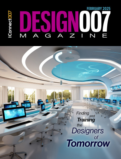
Where will we find the next generation of PCB designers and design engineers? Once we locate them, how will we train and educate them? What will PCB designers of the future need to master to deal with tomorrow’s technology?

The Designer of the Future
Our expert contributors peer into their crystal balls and offer their thoughts on the designers and design engineers of tomorrow, and what their jobs will look like.

Advanced Packaging and Stackup Design
This month, our expert contributors discuss the impact of advanced packaging on stackup design—from SI and DFM challenges through the variety of material tradeoffs that designers must contend with in HDI and UHDI.
- Articles
- Columns
Search Console
- Links
- Media kit
||| MENU - design007 Magazine
J.A.M.E.S. Explores the Future of Additive Manufactured Electronics
February 18, 2025 | Marcy LaRont, I-Connect007Estimated reading time: 1 minute
Andreas Salomon is chief scientist at J.A.M.E.S, a joint venture of Nano Dimension and HENSOLD. In this interview he discusses the evolving landscape of additively manufactured electronics, highlighting the integration of cutting-edge technologies, such as micro-dispensing and ink jetting. These technologies enhance capabilities in signal integrity and miniaturization. He also talks about the importance of sustainability, the need for standardized testing, and collaboration among industry leaders that will drive innovation and transform the future of electronics manufacturing through IPC’s standards development.
Marcy LaRont: Andreas, can you tell me about J.A.M.E.S.?
Andreas Salomon: J.A.M.E.S. stands for Jetted Additively Manufactured Electronics Sources. It is a community and network specialized for additively manufactured electronics in all materials, facades, shades, and processes. We are an online collaboration community with more than 11,000 registered users, and these members are truly working magic in printed electronics. This includes innovations from Nano Dimension, using photopolymers and sintered nanoparticle silver ink, advancements in 3D ceramics, or multi-material projects by AMAREA Technology, a startup we support in Dresden making remarkable progress with ceramic materials.
Joining our community is free. We build our success on strong partnerships that drive innovation and help address industry challenges. J.A.M.E.S bridges the gap between industry needs and requirements, connecting materials and process providers with printer manufacturers.
This is not just a small business case or a killer app. We are advancing research that drives real transformation, reshaping the fundamentals of printed circuit board manufacturing. Our work includes acquiring the necessary qualifications and approvals to turn discoveries into viable products for the future.
To read this entire conversation, which appeared in the February 2025 issue of SMT007 Magazine, click here.
Suggested Items
The Resurgence of European PCB Manufacturing: A Strategic Advantage
02/20/2025 | Jordan Labbe, ICAPE GroupThe global electronics landscape is undergoing a significant transformation. Driven by a confluence of factors, including geopolitical instability, supply chain disruptions, and a growing emphasis on agility and localized production, a renewed focus on European PCB manufacturing is emerging. This resurgence is not merely a trend; it represents a strategic advantage for companies seeking to navigate the complexities of the modern electronics market with multiple sourcing options, outside of China.
STMicroelectronics to Enable Higher-Performance Cloud Optical Interconnect in Datacenters and AI Clusters
02/20/2025 | STMicroelectronicsSTMicroelectronics, a global semiconductor leader serving customers across the spectrum of electronics applications, is unveiling its next generation of proprietary technologies for higher-performing optical interconnect in datacenters and AI clusters.
Revolutionizing Supply Chain: The Cofactr Solution
02/19/2025 | Marcy LaRont, I-Connect007Cofactr was co-founded by Phillip Gulley and Matthew Haber, originally as a small PCB assembly house. Recognizing a greater need, they transformed Cofactr into a supply chain execution platform that automates and optimizes manufacturing processes. The company integrates early design data with supply chain information to identify potential issues, provide risk abatement, and streamline procurement. I met with Phillip at DesignCon and asked him to walk me through the company’s background. He explained how Cofactr helps companies ensure compliance and achieve efficient material management, allowing engineering teams to focus on design rather than logistics.
ODK Media, LG Electronics Sign MOU to Deliver Premium Entertainment Experience on LG Hospitality TVs
02/19/2025 | PRNewswireODK Media has signed a Memorandum of Understanding (MOU) with LG Electronics to enhance premium entertainment experiences on LG Hospitality TVs.
Are Domestic Assemblers Ready for the Next Level of Electronics Miniaturization?
02/19/2025 | Chrys Shea, SHEA Engineering ServicesUHDI technology is more than another evolutionary level of miniaturization. It’s a fundamental change in how we create circuit boards, on a scale potentially as impactful as the transition from through-hole to surface mount was 40 years ago.


