-

- News
- Books
Featured Books
- I-Connect007 Magazine
Latest Issues
Current Issue
From Silos to Systems: 2026 and Beyond
Welcome to the debut issue of I-Connect007 Magazine. This publication brings all of the pieces together from PCB design and fabrication for a closer alignment and a more integrated electronics manufacturing landscape.

Designing Proper Work-Life Balance
In this issue, we hear from designers, marketers, and business owners on how they apply their professional skills to their personal lives to build a healthier work-life balance.

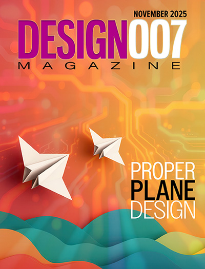
Designing Proper Planes
Without planes, designers would have to create thousands of traces to accomplish the same objectives. Power planes provide low impedance and stable power, and ground planes stabilize reference voltage, improve thermal performance, and help preclude EMI issues.
- Articles
Article Highlights
- Columns
- Links
- Media kit
||| MENU - I-Connect007 Magazine
Elephantech Launches Copper-on-Copper Self-Assembled Nanoparticles
December 22, 2025 | ElephantechEstimated reading time: 1 minute
Japanese deep-tech startup Elephantech Inc. announced the successful development of Self-Assembled Copper Nanoparticles (SA-CuNP), a breakthrough technology that imparts dispersibility to copper microparticle pastes through an entirely new mechanism.
In recent years demand for metal sintering materials has been on sharp rise, especially in the power semiconductor field. Among the metal material candidates, copper pastes, offering lower cost and higher reliability than silver, have shown the most potential.
However conventional copper pastes rely on organic dispersants to stabilize particles, which often leads to reduced metal content, inhibited sintering and lower conductivity, posing limits to broad application.
Elephantech’s SA-CuNP technology overcomes the limitations by enabling copper-to-copper dispersion without depending on organic dispersants.
While previously mechanochemical methods have been introduced to attach one metal particles to the surface of another, now SA-CuNP provides a greatly simplified process: mixing the designated copper nanoparticles with copper microparticles will make the nanoparticles spontaneously assemble into a uniform, continuous layer on the microparticle surface.
SA-CuNP also exhibits a unique behavior: once its concentration exceeds a certain level, self-assembly is rapidly triggered. Elephantech defines the threshold as Critical Self-Assembly Concentration (CSAC), a concept similar to Critical Micelle Concentration (CMC). Above CSAC, dispersion stability increases dramatically, enabling higher-performance paste formulations.
Testimonial
"Your magazines are a great platform for people to exchange knowledge. Thank you for the work that you do."
Simon Khesin - Schmoll MaschinenSuggested Items
PCBAIR Upgrades Heavy-Copper PCBs to Solve AI Thermal Bottlenecks
01/20/2026 | PRNewswireAs computational demands for AI models surge, the hardware powering them faces a critical physical limitation: thermal management.
TÜV Rheinland Advances Electronics Supply Chain Traceability
01/13/2026 | BUSINESS WIREWith electronic devices being replaced at an ever-faster pace, global volumes of consumer e-waste continue to climb.
Elephantech Unveils HDI Microvia Formation Process Using Copper Nanoparticle Ink
12/29/2025 | ElephantechJapanese deep-tech Elephantech announced successful development of an innovative process to form High-Density Interconnect (HDI) microvia leveraging the company’s copper nanoparticle ink, named “Cu Nano Direct Plating.”
TopLine Introduces Cost-Efficient Flip Chips with Daisy Chain for Electrical Test Learning
12/23/2025 | TopLine CorporationFlip Chips with Daisy Chain from TopLine Corporation are a cost-efficient way to learn electrical test for engineers seeking to understand and practice necessary techniques for working with Flip Chip components.
Connect the Dots: The Future of Designing for Reality—Outer Layer Imaging
12/24/2025 | Matt Stevenson -- Column: Connect the DotsIf you read my column regularly, you know I’m passionate about helping designers get the most from their designs. In my November column, I focused on designer best practices for the electroless copper component of the manufacturing process. The next step is outer layer imaging: the transition from digital to physical, and where the designer’s IP meets the board.


