-

- News
- Books
Featured Books
- pcb007 Magazine
Latest Issues
Current Issue
Engineering Economics
The real cost to manufacture a PCB encompasses everything that goes into making the product: the materials and other value-added supplies, machine and personnel costs, and most importantly, your quality. A hard look at real costs seems wholly appropriate.

Alternate Metallization Processes
Traditional electroless copper and electroless copper immersion gold have been primary PCB plating methods for decades. But alternative plating metals and processes have been introduced over the past few years as miniaturization and advanced packaging continue to develop.

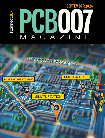
Technology Roadmaps
In this issue of PCB007 Magazine, we discuss technology roadmaps and what they mean for our businesses, providing context to the all-important question: What is my company’s technology roadmap?
- Articles
- Columns
Search Console
- Links
- Media kit
||| MENU - pcb007 Magazine
Ventec, BizLink, Footprintku Announce Strategic Alliance
February 26, 2021 | VentecEstimated reading time: 1 minute
Ventec is pleased to announce that it has entered into a global strategic alliance with leading interconnect solutions provider, BizLink Holding Inc., and Footprintku Inc., an online EDA library and digital transformation services provider for electronic components. This alliance is formed to provide a solution that boosts product development process efficiency and shortens development and time-to-market.
BizLink has long been a supplier of key components to the IT industry, including connectors and cables. The company is experienced in new product introduction (NPI) as well as in system integration, manufacturing, and in assembly.
BizLink’s Chairman, Roger Liang, said, "For the design of electronic products, the trend is for thinner, lighter, and aesthetically pleasing products whilst maintaining functionality and compatibility. This has prompted the demand for rapid and frequent updates of components and product styles. The ability to quickly develop products to respond to market changes has become the key to success."
Ventec International’s Chairman, Tony Lau, pointed out, "What the market needs is a platform that integrates the advantages of upstream components, mid-section design, and back-end manufacturing. The creation of such a platform, we knew, would greatly help accelerate industrial innovation." Footprintku Inc.’s Chairman, YC Hwang, continued, "In response, we propose a cloud platform using the exclusive AI and digital transformation technology of Footprintku.com to integrate the resources of all three companies. The result is a one-stop service, making it possible for product developers to quickly and efficiently find the best components and quality suppliers for their product R&D and design change stages."
This alliance is built upon Footprintku’s cloud database for electronic components as well as BizLink’s solutions and Ventec International’s materials. It integrates the capabilities of new product introduction (NPI), design services (ODM), and manufacturing assembly (EMS). This alliance will reduce the cost of and time in searching for electronic components for product developers. Furthermore, it will accelerate product evolution and facilitate industrial innovation by connecting highly flexible and customized electronic industry supply chain partners.
The alliance was officially announced at a press conference held at the Grand Hyatt Taipei on February 26, 2021.
Suggested Items
Unlocking Advanced Circuitry Through Liquid Metal Ink
10/31/2024 | I-Connect007 Editorial TeamPCB UHDI technologist John Johnson of American Standard Circuits discusses the evolving landscape of electronics manufacturing and the critical role of innovation, specifically liquid metal ink technology, as an alternate process to traditional metallization in PCB fabrication to achieve ever finer features and tighter tolerances. The discussion highlights the benefits of reliability, efficiency, and yields as a tradeoff to any increased cost to run the process. As this technology becomes better understood and accepted, even sought out by customers and designers, John says there is a move toward mainstream incorporation.
Fresh PCB Concepts: The Critical Nature of Copper Thickness on PCBs
10/31/2024 | Team NCAB -- Column: Fresh PCB ConceptsPCBs are the backbone of modern electronics and the copper layers within these boards serve as the primary pathways for electrical signals. When designing and manufacturing PCBs, copper thickness is one of the most critical factors and significantly affects the board’s performance and durability. The IPC-6012F specification, the industry standard for the performance and qualification of rigid PCBs, sets clear guidelines on copper thickness to ensure reliability in different environments and applications.
Book Excerpt: The Printed Circuit Designer’s Guide to... DFM Essentials, Ch. 1
10/25/2024 | I-Connect007The guidelines offered in this book are based on both ASC recommendations and IPC standards with the understanding that some may require adjustment based on the material set, fabricator processes, and other design constraints. This chapter details high-frequency materials, copper foil types, metal core PCBs, and the benefits of embedded capacitance and resistor materials in multilayer PCBs.
The Cost-Benefit Analysis of Direct Metallization
10/21/2024 | Carmichael Gugliotti, MacDermid AlphaCarmichael Gugliotti of MacDermid Alpha discusses the innovative realm of direct metallization technology, its numerous applications, and significant advantages over traditional processes. Carmichael offers an in-depth look at how direct metallization, through developments such as Blackhole and Shadow, is revolutionizing PCB manufacturing by enhancing efficiency, sustainability, and cost-effectiveness. From its origins in the 1980s to its application in cutting-edge, high-density interconnects and its pivotal role in sustainability, this discussion sheds light on how direct metallization shapes the future of PCB manufacturing across various industries, including automotive, consumer electronics, and beyond.
Connect the Dots: Designing for Reality—Pattern Plating
10/16/2024 | Matt Stevenson -- Column: Connect the DotsIn the previous episode of I-Connect007’s On the Line with… podcast, we painted the picture of the outer layer imaging process. Now we are ready for pattern plating, where fabrication can get tricky. The board is now ready to receive the copper traces, pads, and other elements specified in the original CAD design. This article will lay out the pattern plating process and discuss constraints in the chemistries that must be properly managed to meet the customer's exacting manufacturing tolerances.


