-

- News
- Books
Featured Books
- smt007 Magazine
Latest Issues
Current Issue
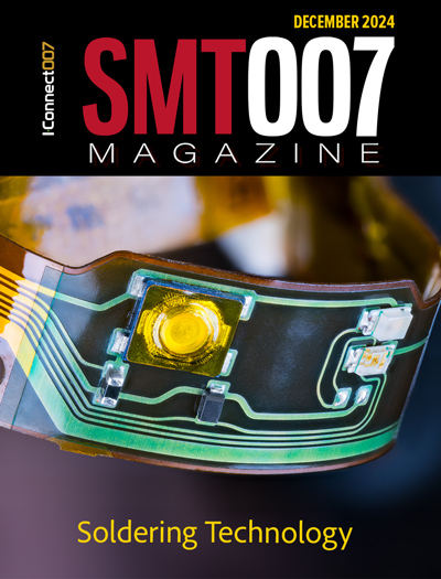
Soldering Technologies
Soldering is the heartbeat of assembly, and new developments are taking place to match the rest of the innovation in electronics. There are tried-and-true technologies for soldering. But new challenges in packaging, materials, and sustainability may be putting this key step in flux.

The Rise of Data
Analytics is a given in this industry, but the threshold is changing. If you think you're too small to invest in analytics, you may need to reconsider. So how do you do analytics better? What are the new tools, and how do you get started?

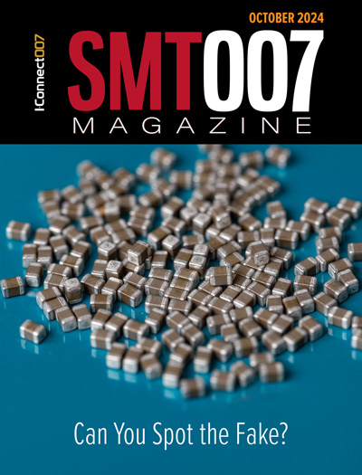
Counterfeit Concerns
The distribution of counterfeit parts has become much more sophisticated in the past decade, and there's no reason to believe that trend is going to be stopping any time soon. What might crop up in the near future?
- Articles
- Columns
Search Console
- Links
- Media kit
||| MENU - smt007 Magazine
Estimated reading time: 4 minutes
Lightning Speed Laminates: Some ‘Exotic’ PCB Processes Could Become Commonplace
Technology is advancing quickly and over the years the PCB industry has advanced its processing and capabilities extensively as well. However, due to technology demands, it is likely that some of the processes for PCB fabrication that were previously considered exotic may soon be considered commonplace. Of course, that prediction depends on many issues. Due to the nature of new and evolving applications, the PCB industry will likely need to make more advances in some of its processing.
Those PCB fabricators who support 77 GHz automotive radar applications are probably very aware of the stringent requirements for these very high frequency applications. Generally, applications at higher frequencies will have more sensitivity to several PCB processes and their normal variations. One simple example is circuit etching quality, and for many mmWave applications, the conductor widths are commonly required to be held to tighter tolerances. The trapezoidal shape of a signal conductor is often specified to be within a certain range and even the roughness of conductor sidewalls have shown to cause RF differences at 77 GHz. Copper plating thickness variation can also be very problematic; having tight control of this process is important for very high frequency applications.
There are several new applications using PCB technology above 77 GHz which require processing capabilities that exceed the current PCB technology. A lot of research work is being done, for example, around 140 GHz for a particular application. The conductor width tolerance needs to be ±1 micron (0.04 mil), conductor thickness needs to be very thin (2 micron), and the thickness variation needs to be at ±0.5 micron. There are some other specifications which are also extremely difficult, or maybe impossible for current PCB technology, such as very tight location tolerances between circuit features and microvias and layer-to-layer alignment.
One of the 140 GHz applications I read about in a white paper on IEEE.org used a combination of PCB technology and semiconductor technology. The main board was made with PCB technology and that circuit board had 35 GHz for the highest operating frequency. That circuit board is no problem for our current PCB fabricators to meet the requirements. However, mounted on the main board was a small glass circuit made with semiconductor technology and that circuit had castellated vias at the edges, which were used to solder-connect to the main board. The 35 GHz signal on the PCB would transition through the castellated vias onto the glass circuit and it would go through a 4x frequency multiplier to get the signal up to ~140 GHz.
After that, the 140 GHz signal would be processed as necessary on the glass circuit. That is a very interesting way to deal with a 140 GHz application, but I would question the capability of high-volume manufacturing as well as cost concerns. If PCB technology can be used to generate circuit features with extreme precision, the high frequency circuit materials that we currently offer can support this technology and have benefits over the glass semiconductor technology.
One PCB technology that has been around for many years is laser-defined conductors. Some of the recent laser technologies can generate high precision circuit geometry. There are limits to these processes currently, but over time, and if the PCB industry develops this technology for high-volume, this could be a process used for the future millimeter-wave PCB circuitry.
Another PCB fabrication process, which may be beneficial for the industry to exert some effort in advancing, is fusion bonding technology. Fusion bonding has been around for many years, but typically not done in high volume manufacturing. There are many things to overcome to make this technology robust for high volume manufacturing while still maintaining the exceptional electrical properties it can offer.
Fusion bonding uses very controlled lamination equipment and processes to basically melt a thermoplastic material, which acts as a bonding material for a multilayer circuit. It will not surprise those engineers who have investigated different high-frequency materials that there is one type of material that stands out for the best electrical performance, especially for very high frequency: PTFE-based material. To laminate a multilayer that uses a PTFE-based bonding material, a fusion bonding process must be used.
A few years ago, Rogers Corporation brought to market a set of PTFE-based materials specifically formulated to meet the electrical needs of very high-speed digital (56 Gbps, 112 Gbps, etc.) applications. The material is Rogers XtremeSpeed RO1200 family of products, and several independent studies have shown this material set can achieve the best electrical performance for very high-speed digital applications.
However, to get the optimum benefit of this material set, the lamination of the multilayer circuit using this material will need to use the XtremeSpeed RO1200 bondply and a fusion bonding process. (As a quick side note, we have achieved very good high-speed digital results when using the XtremeSpeed RO1200 core with SpeedWave 300P prepreg. SpeedWave 300P prepreg does not need fusion bonding and it will have lamination process parameters more common for high-volume PCB fabrication.) A pure package PCB using XtremeSpeed RO1200 core with XtremeSpeed RO1200 Bondply has the best electrical performance for the most demanding high-speed digital applications today. These materials can support the upcoming advanced high-speed digital requirements of the future.
This column originally appeared in the June 2021 issue of Design007 Magazine.
More Columns from Lightning Speed Laminates
Lightning Speed Laminates: Millimeter-wave Properties and PCB Design ChallengesLightning Speed Laminates: Optimizing Thermal Management for Wireless Communication Systems
Lightning Speed Laminates: Test Vehicles for PCB Electrical Material Characterization
Lightning Speed Laminates: Optimum Thermal Stability Considerations
Lightning Speed Laminates: Thermal Management Isn’t Getting Easier
Lightning Speed Laminates: Benefits of High-Performance Hybrid Multilayer PCBs
Lightning Speed Laminates: An Overview of Copper Foils
Lightning Speed Laminates: The Importance of Circuit Features for Millimeter-Wave Applications


