


 Dan’s Biz Bookshelf: ‘Dream First, Details Later
 Happy’s Tech Talk #40: Factors in PTH Reliability—Hole Voids
 Facing the Future: Time for Real Talk, Early and Often, Between Design and Fabrication


Latest Articles
BGA Fanout Routing Overview
PCB developers are deluged with new challenges caused by increasing density and smaller components. Ball grid arrays (BGAs) create particular challenges during layout, with hundreds of connections in just a few square centimeters. Fortunately, designers now have options for addressing these issues.
The Sum of All Parts: Factors of Reliability

A popular definition of reliability is “The quality of being trustworthy or of performing consistently well.” Upfront engineering is of utmost importance in developing a design that will endure its intended life cycle. On the other hand, the manufacturing of that design is just as critical.
PCB Design, Fabrication and Use from the Mil-Aero End-User Perspective

The procedures described for Rolls Royce were directly comparable with those described for MBDA, and the presenters were unanimous in re-emphasising the importance of working closely with their chosen PCB fabricators at all levels and all stages of design, qualification and production of their circuit boards.
Thermal Capabilities of Solder Masks: How High Can We Go?

This article focuses on three different coating material groups that were formulated to operate under high thermal stress and are applied at the printed circuit board manufacturing level. While used for principally different applications, these coatings have in common that they can be key to a successful thermal management concept especially in e-mobility and lighting applications.
Circuit Automation on the Ever-Evolving World of Solder Mask
In a recent conference call, I-Connect007 editorial team was joined by Circuit Automation’s Yuki Kojima, VP of engineering; Larry Lindland, sales and applications manager; and Tom Meeker, CEO, for a lively discussion about solder mask. Spoiler: It’s not all about the equipment.
Countering Solder Mask Residue Production Concerns

The solder mask application is one of the key considerations to ensure a successful application of a selective finish. The selective finish is the final chemical step of the PCB manufacturing process; this is when the panels are at their most valuable and are unfortunately not re-workable.
IMPACT on DIVSYS and NWSC Crane

I-Connect007's Patty Goldman has known DIVSYS’ Stan Bentley for many years, having met when the company was called Diversified Systems and they made circuit boards and finished products at their facility in Indianapolis. They saw each other at IMPACT recently, and of course had to have a chat.
Solder Mask: You’ve Come a Long Way, Baby!
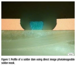
For the July 2018 issue of PCB007 magazine, I-Connect007's editing team met with Electra Polymers’ Shaun Tibbals and Antony Earl to discuss what’s new with solder mask, including direct imaging and inkjet printing of solder mask, and what PCB manufacturers and OEMs need to know.
In With the New at Cadence

The next generation of PCB designers is coming—slowly, but surely. What will this new group of designers mean for EDA vendors like Cadence Design Systems? Andy Shaughnessy recently interviewed Dan Fernsebner, product marketing group director and a veteran EDA guy, and Bryan LaPointe, lead product engineer and representative of the younger generation. They discussed the next generation of PCB designers, some of the best ways to draw smart young people into this industry, and why the PCB designers of the future may need to have a college degree just to get an interview.
More Than a Word: Solder Mask
Do you spend time, as I do, musing on the language of PCBs? We have developed our own lexicon to convey as much by picture, as by word, what exactly we mean.
Calumet Electronics on IMPACT 2018

This year at IMPACT Washington, DC, I-Connect007's Patty Goldman sat down with Steve Vairo and Mike Kadlec of Calumet Electronics, to get their overview on the event.
Study on Application of Four-Wire and Four-Terminal Flying Probe Test Scheme

With the four-wire and four-terminal flying probe test method, voids in the holes formed in the PCB due to process differences, thin copper, and poor conduction due to residual adhesive after laser drilling of the HDI board can be detected, and the circuit board guide can be solved. With the development of multilayer, high-density PCB layout, four-wire four-terminal flying probe testing will play an increasingly important role.
Advanced Copper Plating Process for Any Layer Via Fill Applications with Thin Surface Copper

Copper-filled microvias are a key technology in HDI designs that have enabled increasing miniaturization and densification of printed circuit boards for the next generation of electronic products. Compared with standard PTHs, copper-filled vias provide greater design flexibility, improved signal performance, and can potentially help reduce layer count, thus reducing cost.
Book Review: The Introvert’s Edge

This new book by Matthew Pollard banishes the notion that only extroverts can sell. Gone is the idea that the back slapping, glad handling, joke saying, method of selling is the only way to go.
Agfa: Staying Ahead of the Technology Curve
In the ultracompetitive electronics manufacturing space, companies that don’t continually evolve and invest in new technologies run the risk of being left behind. At the recent EIPC summer conference, many next-generation processes and technologies were discussed and even put on display.
An Owner’s Positive Take on IMPACT 2018: American Standard Circuits’ Founder & Chairman Gordhan Patel
During a full day at IMPACT 2018, I had a chance to speak with American Standard Circuits’ founder and chairman Gordhan Patel. We had much to talk about after listening to several speakers from the departments of Defense and Education, and the International Trade Administration.
Catching up with LiloTree’s Dr. Kunal Shah

Every so often, a new product comes around that promises to be a game changer and LiloTree has one of those products. Not only is it cyanide-free, it has the potential to save 40% on your entire ENIG process and is proving to be far more stable than traditional ENIG products.
Characteristics of New Electroless Au/Pd/Au Process for Fine-Line Applications

The characteristics of electroless gold/palladium/gold (IGEPIG) deposit, which has been newly developed for fine-line application as electroless nickel-phosphorus (EN) free, has been compared with that of conventional electroless Ni-P/Pd/Au (ENEPIG) deposit and electroless Pd/Au (EPIG) deposit.
Welcome to the Silicon Valley Neighborhood: Nano Dimension Arrives in California

I-Connect007 Technical Editor Dan Feinberg accepted an invitation recently to tour Nano Dimension’s new USA headquarters in Santa Clara’s Silicon Valley, which included a sit-down with President and Co-Founder Simon Fried.
Book Review: The Age of Agile—How Smart Companies are Transforming the Way Work Gets Done
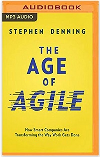
This new book by Stephen Denning addresses the issue of change and adaptability like no other book I have read thus far…and I read a lot of business books! Centering on meeting the challenges of new and often changing business environments and how to meet them, the author’s focus on agility runs from the power of smaller teams that are focused on solving problems quickly while eschewing the normal bureaucratic road blocks that have been in place for decades.
Advanced Stackup Planning with Impedance, Delay and Loss Validation

A typical PCB design usually starts with the material selection and stackup definition—the stackup planning or design exploration stage. How reliable are the data provided by the material vendors and PCB manufacturers? Can we use these data to predict trace width and spacing for the target trace impedance or to calculate delays or evaluate the loss budget?
Susy Webb: Training the New Generation of Designers

For years, I’ve been running into Susy Webb at PCB West, where one of the classes she teaches is PCB design basics. I always ask Susy about the class, especially the attendees’ backgrounds. Over the years, her class has begun drawing more and more degreed engineers, with fewer “traditional” PCB designers attending. I asked Susy to discuss the next generation of PCB designers, some of the trends she’s seeing among new PCB designers, and the need for designers to take charge of their own design training, whether their management agrees or not.
Thermal Management Materials: Easing the Decision-Making Process

There are many different types of thermally conductive materials, and choosing between them will be dictated by production requirements and application design, as well as critical performance factors that must be achieved.
Autocatalytic Gold: How it Fits as a Final Finish

For process sequences or more information regarding semi-autocatalytic gold baths or the latest in the development of a fully autocatalytic gold bath that can eliminate corrosion at thickness of >100 nm please contact the author.
MacDermid Enthone Talks Wet Processing Trends in 2018
I-Connect007’s Patty Goldman, Barry Matties, Andy Shaughnessy, and Happy Holden were recently joined by MacDermid Enthone team members Jordan Kologe, technical marketing specialist; Ted Antonellis, applications manager for electronics specialties; and Don Cullen, marketing director for electronics solutions and MacDermid performance solutions. The discussion topic was the wet processing end of PCB manufacturing.
Copyright © I-Connect007 | IPC Publishing Group Inc. All rights reserved.
Log in