
















 The Right Approach: Old Philosophies, New Tools
 Trouble in Your Tank: HDI and UHDI—Building the Foundation of Advanced Packaging
 It’s Only Common Sense: Look Beyond the Tariffs





Latest Articles
The Use of Insoluble Anodes in Acid Copper Plating

Soluble anodes have been the staple of the industry for decades, but they require extensive maintenance and generate waste in both copper metal and electrolyte. As plated copper thickness uniformity requirements become more stringent, more and more time will be needed for anode maintenance to ensure the uniformity of the anodic setup.
Robert Feranec: A Lifetime of PCB Design
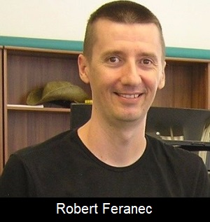
Robert Feranec, a popular YouTuber and founder of the FEDEVEL Academy, discusses with Andy Shaughnessy the upcoming keynote he’ll be giving at AltiumLive in San Diego, California, and how he's helping people around the world understand and optimize their PCB design processes.
Robert Feranec: A Lifetime of PCB Design

I recently spoke with Robert Feranec about the upcoming keynote he’ll be giving at AltiumLive in San Diego, California. Robert is a YouTube star and founder of the FEDEVEL Academy. In our interview, he discusses his keynote presentation as well as how he’s helping designers and engineers around the world understand and optimize their PCB design processes.
EIPC Summer Conference 2019, Day 2

In this article, EIPC Chairman Alun Morgan provides the highlights of the second day of the EIPC 2019 Summer Conference, which was held in the beautiful city of Leoben in central Austria. He also talks about key points of the numerous technical presentation at the conference.
EIPC Summer Conference 2019, Day 1

The beautiful city of Leoben in central Austria provided the setting for the EIPC 2019 Summer Conference. In this article, EIPC Chairman Alun Morgan provides the highlights of the first day of the event, including a recap of the technical presentations.
NCAB 2019 Market Report: Competition Is Heating Up

Chris Nuttall, chief operations officer and VP of technology of NCAB Group, talks about the company's most recently released market report. Nolan Johnson and Nuttall discuss some of the market drivers and conditions the industry can expect to close out in 2019 as well as what to prepare for in 2020.
Selecting the Proper Flex Coverlayer Material

Coverlayers are polymer materials used to cover and protect the copper traces of the flex circuit product. There are a number of different options available for protecting the circuits, and they serve different design requirements in terms of cost, performance, and flexural endurance optimization. When specifying the choice, it is critical to call out not just the type of coverlayer material but also the thickness requirement. This can be very important in certain types of constructions, especially when a flex circuit will experience dynamic flexing during use.
Chemcut: Wet Processing Equipment for the Long Haul

Chemcut CEO and General Manager Rick Lies speaks about the growth he has seen in the marketplace over his 18 years in the industry, and how Chemcut has been able to remain competitive in the PCB and photochemical milling spaces. Jerry Reitz, Chemcut’s HES manager, also addresses the current shift towards zero-discharge facilities.
PCB Design Training: More Critical Than Ever

I interviewed Gary Ferrari of FTG at the IPC High-Reliability Forum and Microvia Summit in Baltimore. Gary is a co-founder of the IPC Designers Council and a longtime advocate for PCB design and PCB designers. We discussed the crucial role that PCB designers play in the entire electronics development process, and how IPC and the Designers Council are helping to educate and inform the next generation of designers.
Putting Green Into a Brownfield Facility

George Milad, national accounts manager for technology at Uyemura, talks about what is driving change in the wet process marketplace and how chemistries must fit into next-generation product design while also meeting new environmental requirements.
The Advantages of Non-sludge Acid Copper Products

Mike Wood, technical director with Cerambus Asia Pacific, discusses the acid copper product from Cerambus Technology Inc. that doesn't generate sludge during the plating process and operates at higher production output by using higher current density. He talks about why this is important for the state of the vertical continuous plating (VCP) market in Asia, and the trends he’s seeing in that space.
The State of Plating

Increasingly, PCB design technology utilises buried and blind via holes and plated via fill is also becoming more and more common. The buried and blind holes mean that the loading on the plating equipment is multiplied by the number of different inner layer connections. The same technology means that equipment needs to deal with thinner and thinner materials.
Meet Mike Hill, I-Connect007 Columnist

Mike Hill has been in the PWB fabrication industry for over 40 years. Throughout his career, he has been a member of IPC and participated in specification writing for both IPC and the military. Within IPC, he has received the President's Award, General Chairmanship, Committee Chairmanship, and many other recognitions. In his columns, Mike will help you better understand the requirements and how-to's for MIL-PRF-31032 certification for PWB fabrication.
Pollution Prevention Techniques: Rinse Water Reduction

There are five general categories of common techniques for pollution prevention in a PCB fabrication facility: new processes to replace sources of pollution; extend the bath’s life; rinse water reduction; dragout reduction; and ventilation reduction. While this list is not all-inclusive, it provides an overview of the types of technologies used around the world that are important to consider. This article, examines rinse water reduction.
Words of Advice: Obstacles to Solid Data Hand-off

In a recent survey, we asked the following question: What are the biggest obstacles you face in getting your design to the fabricator? Here are a few of the answers, edited slightly for clarity.
SAP Utilizing Very Uniform Ultrathin Copper

The demand for miniaturization and higher density electronic products has continued steadily for years, and this trend is expected to continue, according to various semiconductor technology and applications roadmaps. The semiconductor miniaturization brings significant economic and technical benefits and the semiconductor scale factor becomes the master for the associated package and PCB design.
Innovative Electroplating Processes for IC Substrates
The decreasing chip scales and smaller line/spacing distances have created unique challenges for both the PCB industry and the semiconductor industry. This paper discusses innovative additive packages for direct-current copper electroplating specifically for IC substrates, which offer better trace profile and deliver via fill and through-hole plating. It also describes two electrolytic copper plating processes, the selection of which could be based on the via size and the dimple requirements of the application.
Vertical Conductive Structures, Part 3: Design Tool Techniques
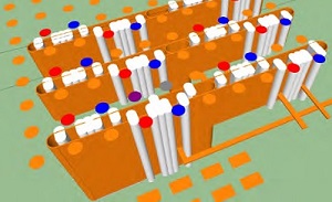
New vertical conductive structure (VeCS) technology can reduce layer count and improve signal integrity without the need for sequential technologies. VeCS is different than traditional through-hole vias, microvias, and ELIC designs, which are more expensive and require a high number of laminations, drilling, and plating cycles to build up a reasonable number of layers.
Words of Advice: Your Company’s Design Process
In a recent survey, we asked PCB designers to describe their company’s design process: Is it a rigid workflow they follow to the letter, or a process that allows for their individual techniques? Of course, the comments were illustrative.
Nano Dimension Details New DragonFly LDM
Dan Feinberg talks with Nano Dimension CEO Amit Dror about the new DragonFly LDM 3D printer technology announced by the Israeli company on July 24, 2019, aimed at increasing machine uptime and moving forward from prototyping to higher production volumes.
Bill Brooks on Teaching PCB Design at Palomar College

Bill Brooks of Nordson ASYMTEK is a long-time PCB designer and one of the first people to teach PCB design courses in a college setting. He recently spoke with the I-Connect007 editorial team about his history in design and his time as a PCB design instructor, the curriculum he developed and taught, and various techniques that might be enacted today to better educate the designers of tomorrow.
Solder Mask Curing: UV Bump Overview

Ultraviolet (UV) bump, also called UV cure, is a processing step in which the solder mask pattern is irradiated with ultraviolet and infrared light. This step is performed with special equipment that is built as a continuous flow system, which consists of a conveyor belt and tubular UV lamps mounted above and below the belt. Read on to find out more about this process.
There’s An Art to Plating

There's definitely an art to plating. Start with a generally planar substrate, then alternately put stuff on and take things off. Continue this in subtle variations until what you have is the stuff you want, where you want.
Words of Advice: Drawbacks to Your PCB Data Format?
In a recent survey, we asked the following question: What is the biggest drawback to your current PCB data format? Here are a few of the answers, edited slightly for clarity.
Development of Flexible Hybrid Electronics
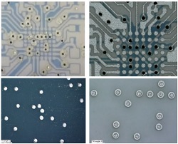
This article will present a hybrid manufacturing process to manufacture FHE systems with a two-layer interconnect structure utilizing screen printing of silver conductive ink, filled microvias to connect ink traces at the different layers, and use of the traditional reflow process to attach the semiconductor chips to the printed substrates.
Copyright © I-Connect007 | IPC Publishing Group Inc. All rights reserved.
Log in